About Us
A high-technology enterprise specializing in semiconductor packaging and testing
One-Stop SiP (System-in-Package) Solution Development Platform
Shanghai Liyuan Micro Semiconductor Co., Ltd. is a professional SiP (System-in-Package) solution development platform. For years, the company has been providing customers with integrated one-stop services and solutions, including ASIC chip design, SiP packaging design and simulation, wafer sourcing for internal SiP assembly, SiP production, system-level testing, reliability and failure analysis. The company's flagship product — Chiplet/SiP system-level chips — has achieved cumulative shipments of over 100 million units, exclusively serving the domestic market with professional expertise.
Focusing on advanced packaging technologies in semiconductor integrated circuits, MEMS, and optics, the company continues to build high-end R&D platforms and is committed to providing SiP chip customization support for domestic microsystem enterprises. This helps customers lower R&D barriers and upfront costs while effectively shortening product development cycles.
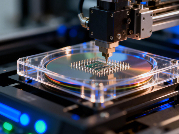
Shanghai Liyuan Micro Semiconductor Co., Ltd. operates its packaging base in Nanjing, which features a high-specification cleanroom of over 2,200 square meters. Equipped with industry-leading packaging and testing equipment, the facility offers full-process capabilities, including wafer testing, thinning, dicing, chip mounting, molding, marking, ball placement, electromagnetic shielding, singulation, reliability testing, failure analysis, functional testing, and packaging.
The company holds technical advantages in high-precision surface mounting of ultra-thin passive components and multiple heterogeneous chips, providing advanced packaging solutions for complex, high-density mounting surfaces. Its complete process portfolio includes sputter-based EMI electromagnetic shielding technology. The technology platform specializes in advanced system-level packaging processes such as FC SiP, FC+WB SiP, SiP modules, Stack Die SiP, fcFLGA, fcFBGA, fcPoP, LGA, and FBGA. It offers partial or fully customized, one-stop system-level packaging and testing services for chips including MEMS, ASICs, microprocessors, memory, power management ICs, and wireless communication ICs across various product applications.