SiP/Chiplet Packaging Manufacturing
SiP/Chiplet Packaging Manufacturing
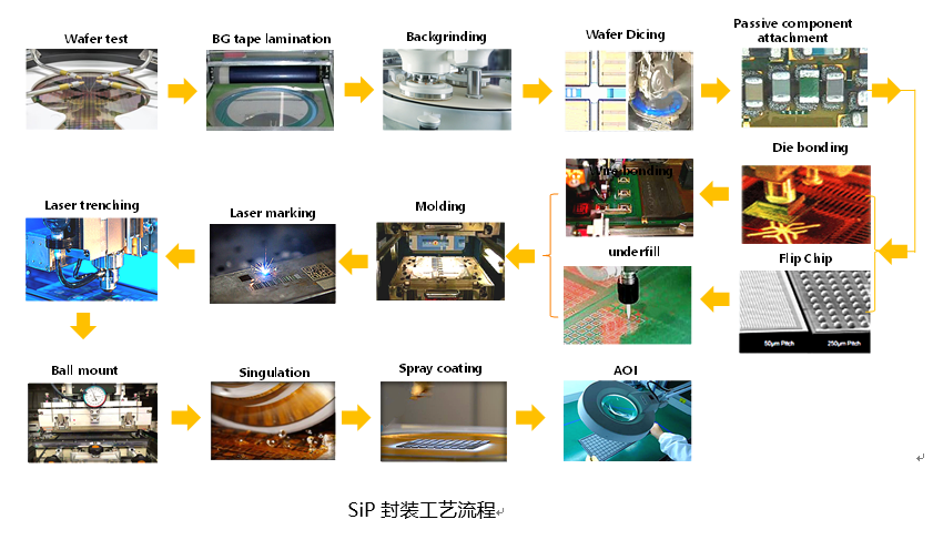
As illustrated below, our production flow spans wafer test through AOI inspection, enabling rapid prototyping and low-volume production for our customers.
By process sequence, production is organized into three stages: front-end, mid-end, and back-end.
(1) Front-End Processes Include wafer test, wafer thinning, and dicing—covering IC wafer CP (chip probe) test, full cut, and half cut, as well as MEMS wafer CV test and stealth laser dicing. Wafer thinning processes are selected based on die type and thickness requirements, including grind-then-dice or half-cut-then-grind flows.
(2) Mid-End Processes Include passive component placement, face-up die attach, wire bonding, flip-chip assembly, underfill, and related steps. Capabilities span high-density SMT placement, standard and fine-pitch flip-chip processes, 2.5D/3D die stacking, and CUF versus MUF selection.
(3) Back-End Processes Include molding, laser marking, EMI shielding, BGA ball attach, singulation, AOI inspection, and related steps. Capabilities include full mold and selective mold, compartment shielding and conformal shielding, automated and manual ball attach, and standard and irregular singulation.