System-in-Package Design
1. Introduction to System-in-Package (SiP)
SiP (System-in-Package) refers to the integration of multiple active electronic components with different functions, along with optional passive devices and other components such as MEMS or optical devices, into a single standard package that achieves a specific function, thereby forming a system or subsystem.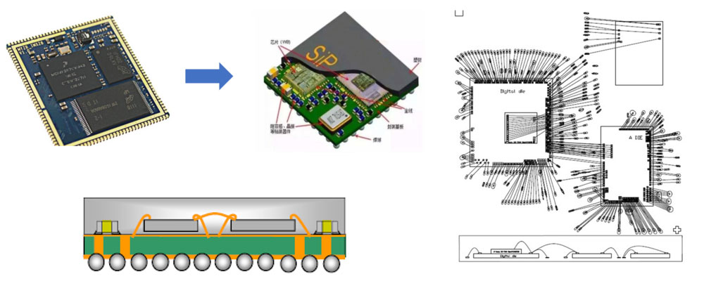
2. SiP Package Design
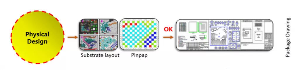
Based on specific SiP solution requirements, and taking into account subsequent substrate and assembly process rules, we carry out device placement, package stacking, substrate layout, and package pinmap optimization. We then output substrate Gerber files, package bonding diagrams (BD drawings), strip panelization, POD (Package Outline Drawing), and other engineering documents to downstream substrate or process teams for assembly and production.
3. SiP Package Simulation and Optimization
Electrical simulation analysis:
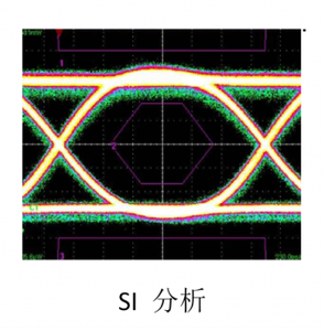
Includes S-parameter extraction, crosstalk analysis, SSO analysis, eye diagram analysis, capacitance normalization, power current distribution and DC IR-drop analysis, package EMC analysis and optimization, and die-PKG co-simulation, etc.
(1) Signal Integrity (SI) Analysis
· Package RLC parameter extraction: Extracts RLC parameters to obtain an equivalent circuit model of the package;
· TDR analysis of signal networks: Obtains the characteristic impedance of package routing in different regions and identifies impedance mismatch areas;
· S-parameter extraction of signal networks: Evaluates whether signal quality meets electrical performance requirements based on insertion loss and return loss;
· Signal isolation analysis: Determines whether crosstalk specifications are met by analyzing near-end and far-end crosstalk between different signals;
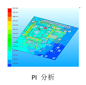
(2) Power Integrity (PI) Analysis
· DC IR-drop analysis: Analyzes DC voltage drop across power networks inside the package and optimizes networks that do not meet specifications;
· Current density analysis: Analyzes current density in power-ground networks inside the package and optimizes areas exceeding specifications;
· AC impedance analysis of power networks: Analyzes self-impedance of power networks, evaluates whether target impedance is met, and provides capacitor optimization solutions;
· Resonance analysis: Analyzes resonant frequency, location, and amplitude of power-ground planes inside the package;
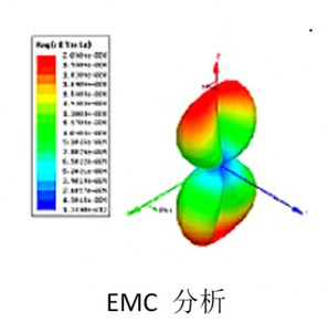
(3) Electromagnetic Compatibility (EMC) Analysis
Analyzes whether the electromagnetic field distribution on the package and PCB meets electromagnetic shielding requirements and provides EMC optimization solutions.
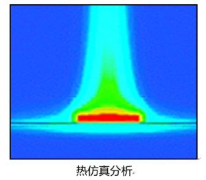
Thermal Simulation Analysis: Performs thermal design simulation for devices/modules with heat dissipation requirements.