Advanced Packaging Technology Decoded | TSMC: The "Master Architect" of the Chip World
When smartphones run ever smoother, large AI models operate at lightning speed, and gaming graphics card computing power surges, behind it all lies TSMC's "hidden ace"—advanced packaging technology.
If chip manufacturing processes are the "art of microscopic sculpting," then advanced packaging is the "master architect of chips," assembling individual small chips into computing monsters that send performance soaring and power consumption plummeting, shouldering half the computing power of the AI era!
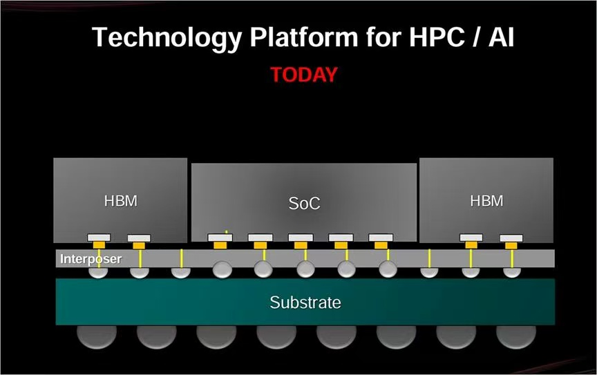
I. Why Is Advanced Packaging So Important?
Traditional chips are like "lone wolf" all-rounders—they must compute fast, store a lot, and stay small. As they push further, breaking through physical limits becomes increasingly difficult (Moore's Law slowdown).
Advanced packaging adopts a different mindset: break the whole into parts and assemble them like building blocks! Chips are dismantled into computing, storage, communication, and other "small blocks," then tightly "bonded" together using specialized techniques, preserving their individual strengths while enabling high-speed collaboration, achieving a "1+1>2" effect.
And TSMC is the master who has perfected this "art of building blocks," leveraging its 3DFabric® technology portfolio to firmly lock down the global packaging market for high-end AI chips and premium smartphone chips.
II. TSMC's Three Ace Packaging Technologies, Explained Simply
1. CoWoS: The "Super Highway" for AI Chips (2.5D Packaging)
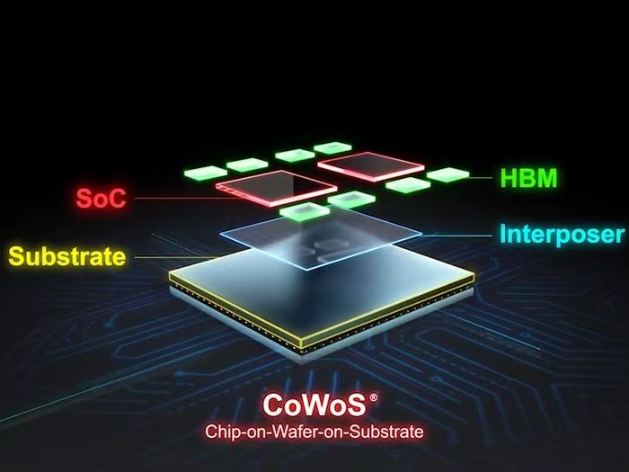
CoWoS (Chip on Wafer on Substrate) is TSMC's "signature move," arguably the exclusive "luxury villa" for AI chips.
• Core Principle: An ultra-thin silicon wafer serves as a "super circuit board" (silicon interposer), on which chips like GPU and HBM (High Bandwidth Memory) are laid side by side and connected via nanoscale wiring.
• Simple Analogy: Communication between chips in traditional packaging is like "taking a country road"—slow and prone to jams; CoWoS builds a "bi-directional 100-lane expressway,"
shrinking signal transmission distance to the micron scale, achieving near-zero latency and maxed-out bandwidth (e.g., NVIDIA's H100 GPU relies on it for 5.3TB/s of memory bandwidth).
• Application: Top-tier AI GPUs like NVIDIA H100/H200 and AMD MI300 all depend on CoWoS for survival.
2. SoIC: The "Master of Stacking" for Chips (3D Packaging)
If CoWoS is a "planar expressway," then SoIC (System on Integrated Chips) is a "three-dimensional skyscraper"—TSMC's most cutting-edge 3D packaging technology.
• Core Principle: Abandoning traditional solder balls, chips are directly stacked vertically "face-to-face" or "face-to-back" like a human pyramid, shrinking inter-chip spacing to 6 microns (with plans to further reduce it to 4.5 microns), causing interconnect density to skyrocket.
• Simple Analogy: Replacing the "expressway" with a "vertical elevator," chips communicate directly top-to-bottom, enabling faster data transfer, lower power consumption, and smaller chip dimensions.
• Application: AMD high-end processors, Apple A-series chips, and the "memory stacking" of future AI chips all rely on it to boost computational density.
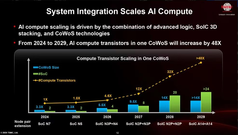
3. InFO: The "Value King" for Mobile Chips
InFO (Integrated Fan-Out) is TSMC's "lightweight packaging" tailored for mobile devices like smartphones and tablets, prioritizing "small, thin, and cost-effective."
• Core Principle: Without a silicon interposer, a redistribution layer is created directly on the wafer to "fan out" the chip pins, simultaneously shrinking chip area and reducing cost.
• Simple Analogy: A "slim-down and burden-relief" plan for mobile chips, making phones thinner and lighter with better heat dissipation, all while controlling costs—truly the "cost-effective choice" for mobile chips.
• Application: Mainstream mobile chips like Apple A-series and MediaTek Dimensity series are inseparable from InFO technology.
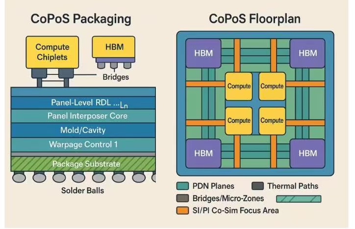
III. Next-Gen Black Technology: CoPoS, "Turning Round into Square" to Break Limits
As AI chips grow ever larger, traditional CoWoS uses a round wafer substrate, which limits area, incurs high costs, and is prone to warping.
TSMC unveils its CoPoS (Chip-on-Panel-on-Substrate) masterstroke: replacing the round wafer with a large square panel!
• Material utilization rate doubles, capacity significantly increases, and costs drop;
• Larger panel size accommodates more and bigger chips, meeting the demand for future ultra-large AI chips.
Pilot production has begun, with mass production expected by 2028; NVIDIA is likely to be among the first customers.
IV. How Does TSMC Monopolize Advanced Packaging?
1. High Technical Barriers: From launching CoWoS in 2011 to the current full-stack 3DFabric layout, rapid technological iteration and a vast patent portfolio leave competitors struggling to catch up;
2. Exclusive Capacity: Global high-end CoWoS capacity is almost entirely monopolized by TSMC, with giants like NVIDIA, AMD, and Apple queuing up to place orders; even having money doesn't guarantee capacity;
3. Full-Stack Integration Capability: Able to deliver both cutting-edge processes like 3nm and 2nm and top-tier packaging—the powerful combination of "process + packaging" maximizes performance.
V. Summary: Advanced Packaging, TSMC's "Second Moat"
Today, as Moore's Law slows, advanced packaging has risen to equal footing with advanced process technology, becoming TSMC's second moat.
From the slim-yet-powerful efficiency of mobile chips, to the computing surge of AI GPUs, and on to the performance breakthroughs of future super-scale models, TSMC wields its three aces—CoWoS, SoIC, and InFO—
alongside the next-gen CoPoS black technology, firmly controlling the discourse in advanced packaging and continuously injecting "core" momentum into the global chip industry!
Shanghai Liyuan Micro Semiconductor Co., Ltd. is a professional SiP system-in-package solution development platform. For many years, we have provided customers with one-stop services and solutions, including ASIC chip design, SiP packaging design and simulation, SiP internal wafer procurement, packaging production, system-level testing,
reliability and failure analysis, and more. Our company offers free SiP/Chiplet design consultation and services to all customers, dedicated to helping clients achieve design goals such as small form factor, low power consumption, and low cost.
If interested, please feel free to contact us at +86 13817180836 (same number for WeChat).