Post-Moore Era: Chip "Magic Stacking" – A Super Cool Integration Technology Adventure
As the chip's "shrinking act" reaches its limit and transistors approach the physical "ceiling," the pace of Moore's Law gradually slows – but the semiconductor legend is just opening its most exciting chapter!
In the post-Moore era, engineers are no longer obsessing over "smaller," but are instead playing with "smarter": treating chips like building blocks, puzzles, or even magical castles, using wildly imaginative integration technologies to keep computing power, speed, and performance soaring.
Today, let's use the most vivid language to unpack these "black tech magic tricks" hidden within fingernail-sized spaces!
I. Moore's Law "Retires," the Chip World Welcomes New Gameplay
Once upon a time, chip evolution relied on "squeezing": every 18 months, transistors were made smaller and smaller, packed onto the same silicon die, doubling performance and halving cost.
But today, 3nm and 2nm processes are more precious than gold, the design cost of a 5nm chip has skyrocketed to $500 million, and if transistors get any smaller, they'll start to "fight" with quantum tunneling – leakage, heat, and costs are exploding – the single-chip path has reached its end.
Thus, the industry has collectively "changed lanes":
From "one chip does it all" to "multiple chips team up for advantages";
From "spreading flat like a pancake" to "stacking vertically like a skyscraper";
From "obsessing over a single material" to "mixing multiple materials."
This is the core of the post-Moore era: using the "cleverness" of packaging and integration to break through the "brute force" limits of process nodes, allowing chip performance to continue taking off while keeping costs firmly grounded.
II. Chiplet: The "LEGO Master" of the Chip World, Piecing Together Unlimited Possibilities
If a traditional chip is a "whole cake," then Chiplet is cutting that cake into "small pieces" – CPU, GPU, memory, interfaces, AI engines – each made into an independent small chiplet, then precisely assembled together like LEGO bricks.
• Why is it so appealing?
No need to make a "super-large chip" (difficult, expensive, prone to failure); small chiplets have clear divisions of labor – if one breaks, replace just that one – costs are greatly reduced;
Different processes and materials can be mixed and matched: use advanced processes for compute chiplets, mature processes for interface chiplets – complementary advantages, 1+1>2;
R&D cycles are cut in half; to upgrade, just swap one piece – incredibly flexible.
• How popular is it?
High-end AI chips and server CPUs all rely on it to "stay alive." The global market is projected to grow from $2.4 billion in 2023 to $21.5 billion in 2028 – nearly a ninefold increase.
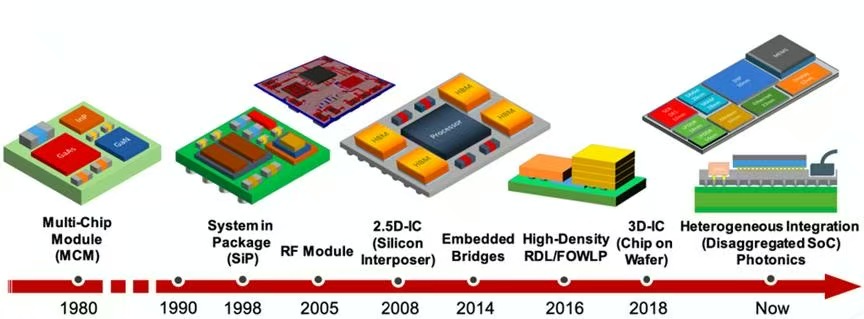
III. 2.5D Packaging: The "Super Highway" Between Chips, Speed Soaring
For Chiplets to assemble quickly, the "connections" need to be powerful enough – 2.5D packaging is like building a "silicon-based highway" for the chiplets.
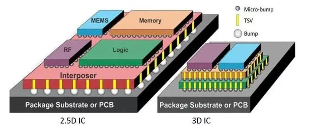
Between the chip and the substrate, a super-thin silicon interposer is hidden, filled with micron-scale ultra-fine wiring and TSV (Through-Silicon Vias) – like drilling "vertical tunnels" through the chip.
• Magical Effects:
GPU and HBM (High Bandwidth Memory) sit "shoulder to shoulder," their data channel transforming from a "country lane" into a "16-lane superhighway," with bandwidth soaring to TB/s levels;
Interconnect length shrinks from millimeters to micrometers, latency plummets, power consumption drops by 90% – it's the "standard base" for high-end AI computing power.
IV. 3D Stacking: The "Stacking Game" of the Chip World, Maximizing Space Utilization
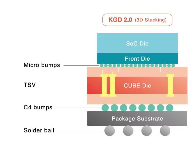
Not satisfied with just planar assembly? Stack them up! 3D packaging vertically layers chips one on top of another, bonding them together with TSV + hybrid bonding.
• Traditional vs. 3D:
Traditional: Chips laid out flat – long connections, slow speed, take up lots of space;
3D: Compute chips stacked on memory chips, AI chips stacked on logic chips – density increases several times, volume shrinks by half.
• Black Tech Upgrade: Hybrid Bonding
No solder needed – copper contacts on chips are directly "fused face-to-face," with bonding pitch entering the sub-micron range, interconnect density exploding – the "ultimate form" of future 3D packaging.
V. SiP (System-in-Package): A "Mini Supercomputer" in Your Pocket
Tight space in phones, watches, earbuds? SiP (System-in-Package) directly packs CPU, memory, sensors, and RF chips into a single small housing – one package is a complete system.
• What's the magic?
Extremely small footprint, shorter wiring, lower interference – the "destined technology" for smart wearables and IoT devices;
No need to redesign chips – quickly integrate functions, directly shortening R&D cycles.
VI. Future Black Tech: Glass Substrates + Co-Packaged Optics, Science Fiction into Reality
Think current tech is already cool? Even more mind-blowing things are yet to come:
• Glass Substrate Packaging
Say goodbye to organic substrates that are prone to warping and signal loss – glass material is as stable as a rock, allows finer wiring, and has extremely low signal loss – the "ideal stage" for ultra-large bandwidth chips.
• CPO (Co-Packaged Optics)
Pack the "optical engine" directly inside the chip package – use electrical signals for computing, optical signals for data transmission – latency reduced by 90%, power consumption cut in half – the "future destiny" for data centers and supercomputing.
VII. Final Thoughts: The Magic of Integration Has Just Begun
Moore's Law may have slowed, but chip innovation has never stopped.
The post-Moore era is not the endpoint of performance, but the golden age of integration technology – the flexibility of Chiplets, the speed of 2.5D, the compactness of 3D, the small size of SiP, plus the added advantages of optics and new materials.
From mobile phones to AI servers, from automotive electronics to aerospace chips, these "magical integration techniques" are making every chip stronger, smaller, and smarter.
The next time you pick up your phone and experience lightning-fast computing power, don't forget: hidden beneath your fingernail is not just transistors, but humanity's most romantic display of wisdom – packing infinite possibilities into a tiny space.
This chip integration celebration has just begun to unfold!
Shanghai Liyuan Micro Semiconductor Co., Ltd. is a professional SiP system-level packaging solution development platform. For many years, we have provided customers with one-stop services and solutions including ASIC chip design,
SiP packaging design and simulation, wafer procurement for internal SiP use, packaging production, system-level testing, reliability and failure analysis.
Our company offers free SiP/Chiplet design consulting and services to all customers. We are dedicated to helping customers achieve design goals such as small form factor, low power consumption, and low cost.
If interested, please feel free to contact us at 13817180836 (WeChat ID same as phone number).