Understanding Chip Packaging
I. Basic Concepts of Packaging
1. What is Packaging?
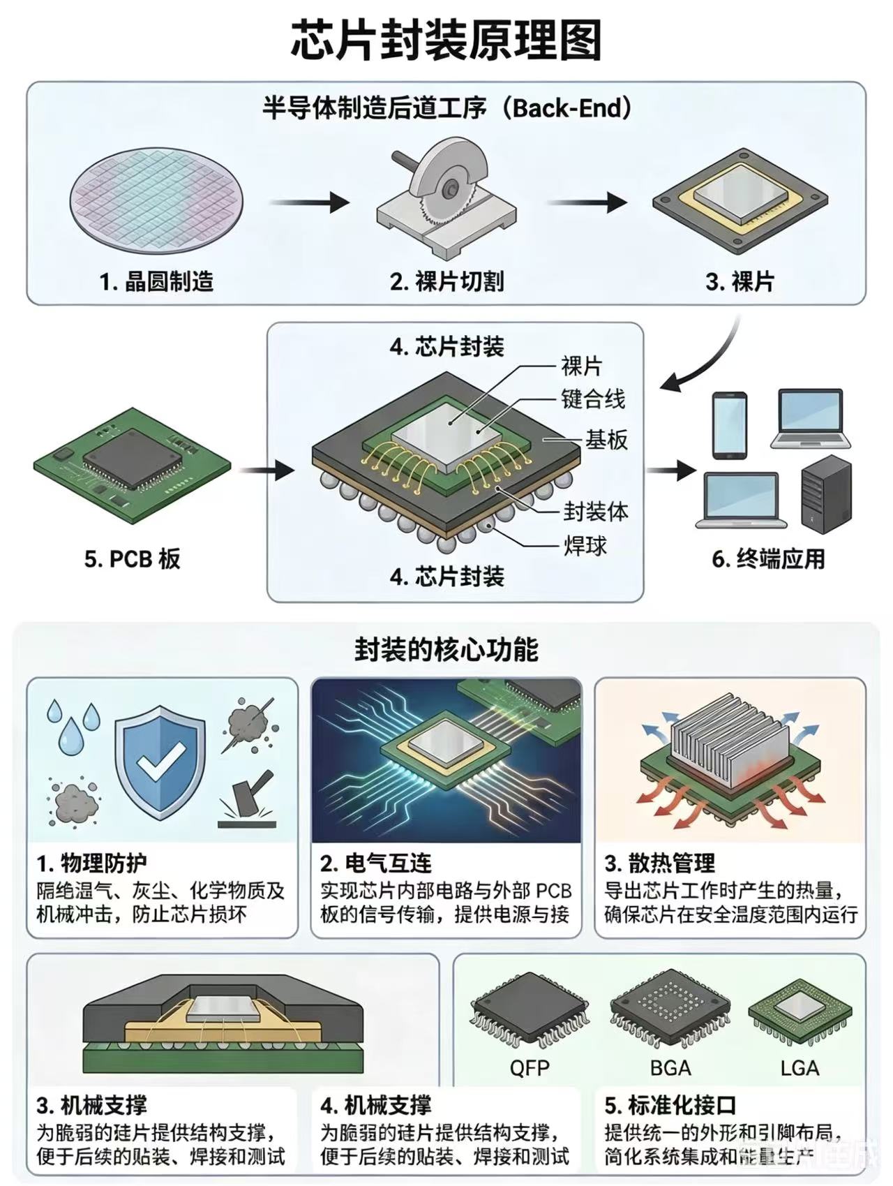
Chip packaging is a back-end process in semiconductor manufacturing. It is a critical step that puts a "protective coat" on the bare die after wafer dicing and establishes electrical connections between the chip and external circuits.
2. Complete Process from Wafer to End Product
1. Wafer Fabrication → 2. Die Dicing → 3. Bare Die → 4. Chip Packaging → 5. Soldering to PCB → 6. End Application (Mobile Phone/Computer/Server, etc.)3. The 5 Core Functions of Packaging
Function Core Role
Physical Protection Isolates moisture, dust, chemical corrosion, and mechanical shock to protect the fragile silicon die
Electrical Interconnection Enables signal transmission between the internal chip circuit and the external PCB, providing power/ground paths
Thermal Management Dissipates heat generated by the chip during operation, preventing performance degradation or damage due to overheating
Mechanical Support Provides structural support for the silicon die, facilitating subsequent mounting, soldering, and testing
Standardized Interface Offers a uniform form factor and pin layout, simplifying system integration and mass production
II. Key Packaging Components and Materials
Component/Material Core Role Common Types/Materials
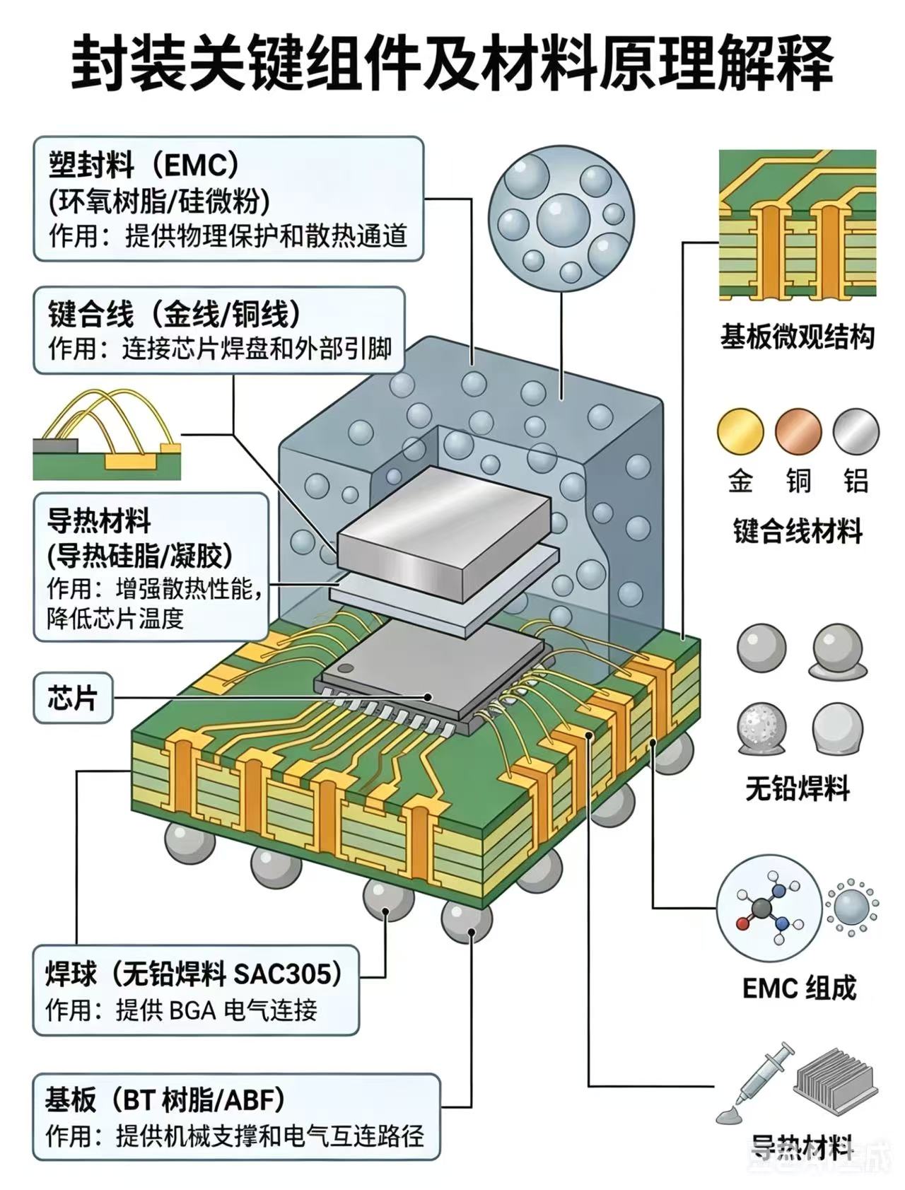
Die Core functional unit, the bare die after wafer dicing -
Substrate Provides mechanical support and electrical interconnection paths BT Resin/ABF Substrate
Bonding Wire Connects chip pad to external lead, enabling electrical signal transmission Gold wire, Copper wire, Aluminum wire
Molding Compound (EMC) Physical protection, also assists in heat dissipation Epoxy resin + Silica filler
Thermal Interface Material Enhances heat dissipation, reduces chip temperature Thermal grease, Gel
Solder Ball Provides electrical connection for BGA packages Lead-free solder (e.g., SAC305)
III. Chip Packaging Process Flow (9 Steps)
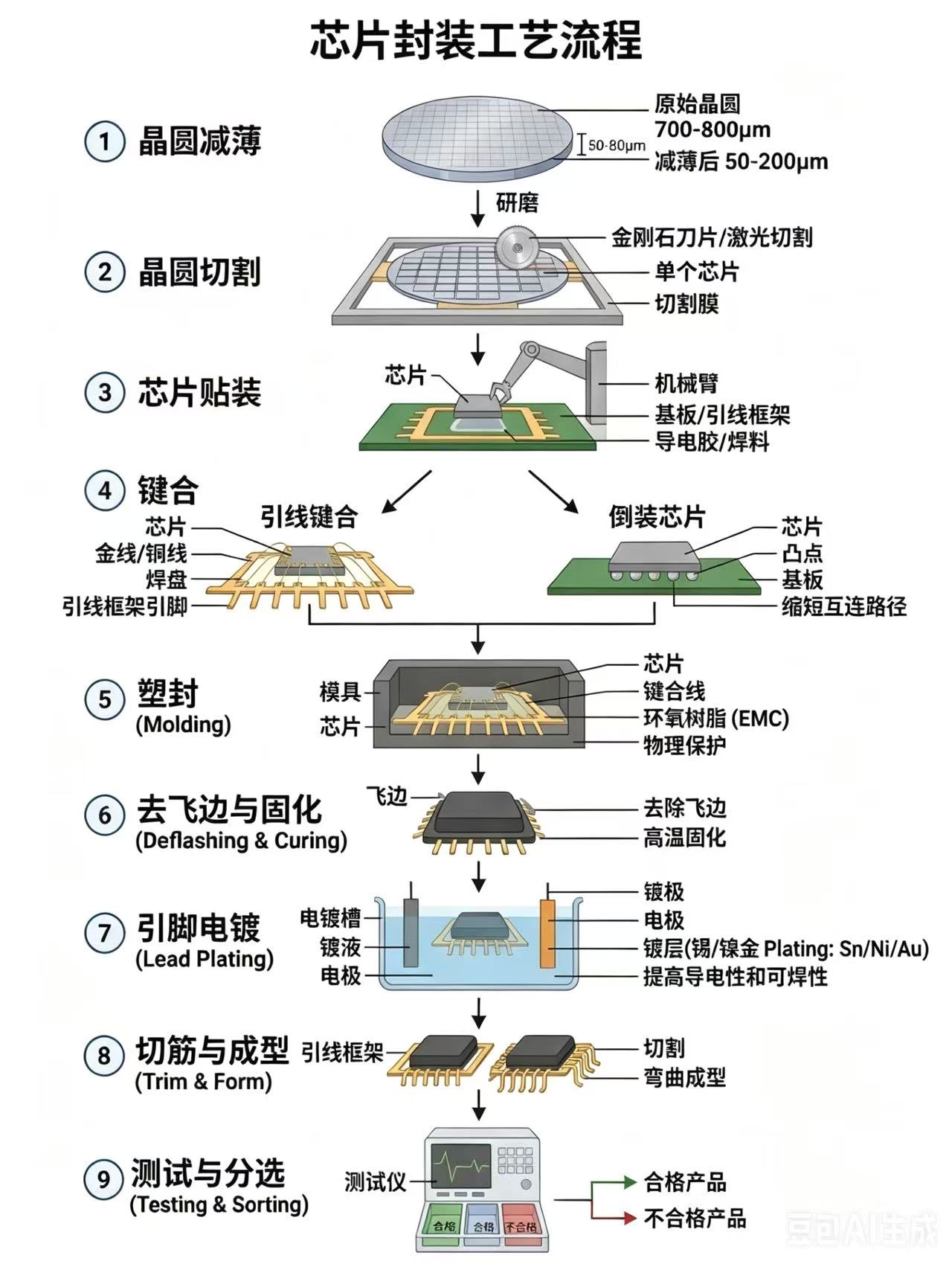
1. Wafer Thinning: The original wafer is ground down from 700-800μm to 50-200μm in preparation for subsequent dicing and heat dissipation.
2. Wafer Dicing: A diamond blade or laser is used to separate the wafer into individual bare dice.
3. Die Attach: A robotic arm fixes the bare die onto a substrate/lead frame using conductive adhesive or solder.
4. Bonding:
◦ Wire Bonding: Uses gold/copper wires to connect chip pads to leads – a mature process
◦ Flip Chip: Directly connects chip bumps to the substrate for shorter paths and better performance
5. Molding: Epoxy molding compound (EMC) encapsulates the chip and bonding wires, providing physical protection.
6. Deflash and Post-Mold Cure: Removes excess material from the molding process and cures the epoxy resin at high temperature.
7. Lead Plating: Leads are plated with tin/nickel/gold (Sn/Ni/Au) to improve conductivity and solderability.
8. Trim and Form: Finished units are cut from the lead frame, and leads are bent into their final shape.
9. Test and Sorting: Test equipment is used to screen pass/fail units; passing units are shipped to market.
IV. Five Generations of Packaging Technology Evolution
Generation Time Representative Technologies Key Features
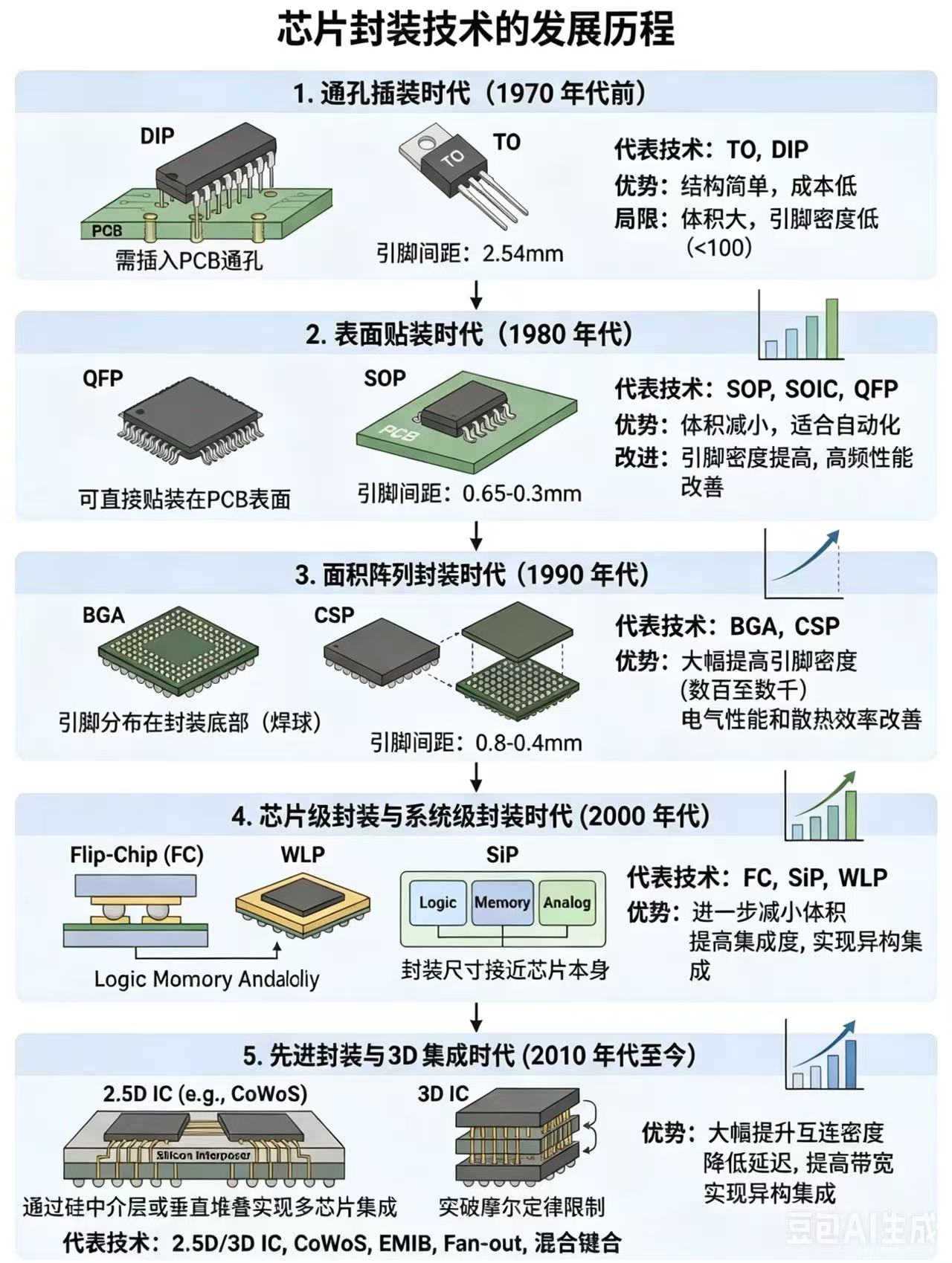
1. Through-Hole Era Pre-1970s TO, DIP Pins are inserted through holes in the PCB; simple structure, low cost; but large size, low pin count (<100)
2. Surface Mount Era 1980s SOP, SOIC, QFP Mounted directly on PCB surface; reduced size, suitable for automation; improved pin count and high-frequency performance
3. Area Array Era 1990s BGA, CSP Pins (solder balls) are distributed across the bottom of the package; pin pitch reduced to 0.8-0.4mm; significantly higher pin density, improved thermal and electrical performance
4. Chip-Scale/System-in-Package Era 2000s FC, SiP, WLP Package size approaches the size of the chip itself; further reduces volume, increases integration density, enables heterogeneous integration
5. Advanced Packaging and 3D Integration Era 2010s–present 2.5D/3D IC, CoWoS, EMIB, Fan-out, Hybrid Bonding Greatly increases interconnection density, reduces latency, increases bandwidth, pushes beyond Moore's Law limits,
enables multi-chip integration
Shanghai Liyuan Micro Semiconductor Co., Ltd. is a professional SiP system-level packaging solution development platform. For many years, we have provided customers with one-stop services and solutions including ASIC chip design,
SiP packaging design and simulation, wafer procurement for internal SiP use, packaging production, system-level testing, reliability and failure analysis.
Our company offers free SiP/Chiplet design consulting and services to all customers. We are dedicated to helping customers achieve design goals such as small form factor, low power consumption, and low cost.
If interested, please feel free to contact us at 13817180836 (WeChat ID same as phone number).