Comprehensive Analysis of Advanced Packaging Integration Technology
Comprehensive Analysis of Advanced Packaging Integration Technology: Technical Logic and Evolution Path of Chiplet and Heterogeneous Integration
I. Core Background: The Inevitable Choice in the Post-Moore Era
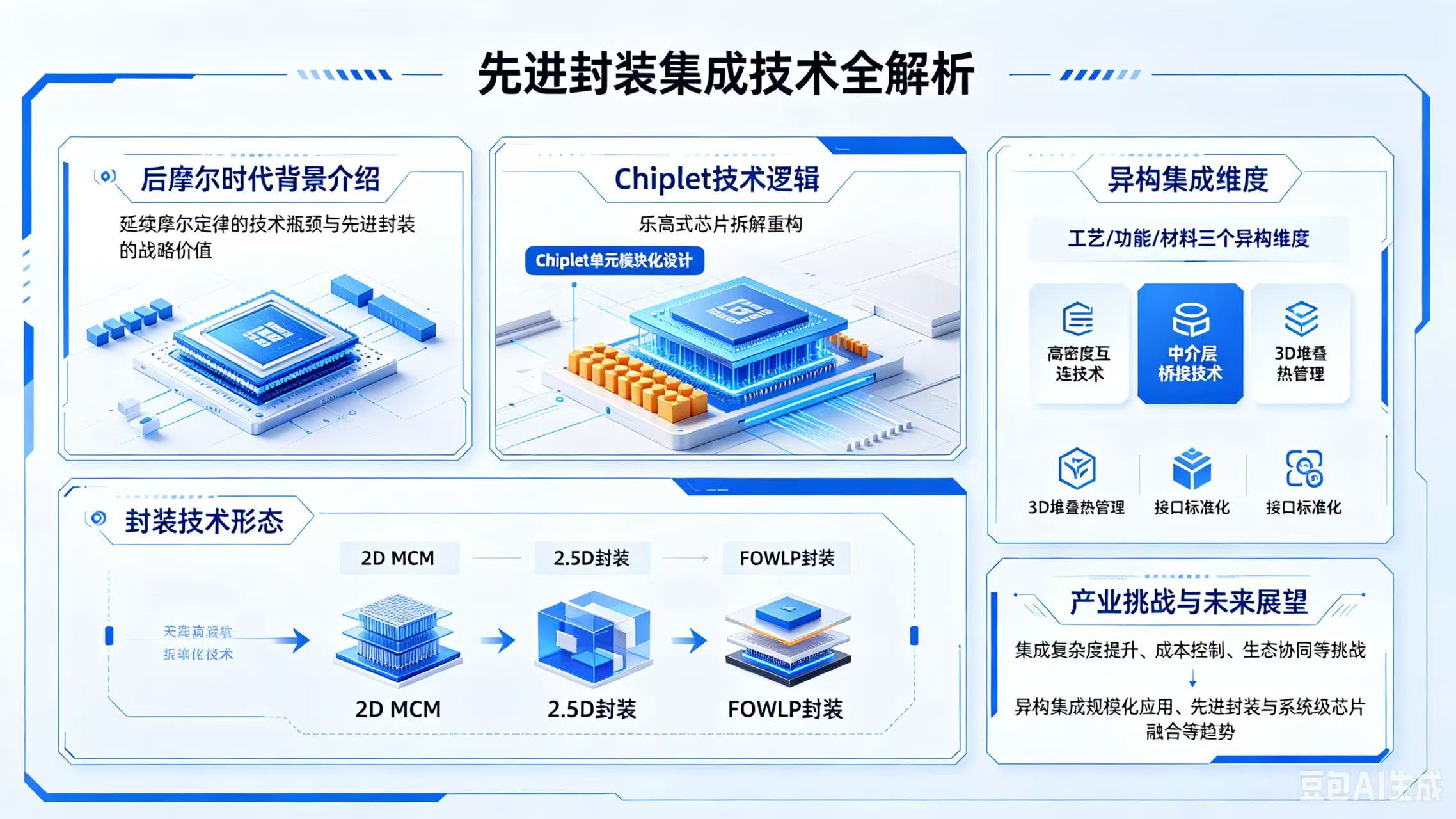
As Moore's Law slows down (process nodes approach 2nm and below, physical limits become prominent), single-chip area is constrained (reticle limit, sharp decline in yield), and computing power demand soars (AI/data centers/autonomous driving),
advanced packaging (Chiplet + Heterogeneous Integration) has become the core path to break through performance, cost, and yield limitations, shifting from "transistor scaling" to "system-level integration innovation."
II. Chiplet Technology: The "Lego-like" Chip of Deconstruction and Reconstruction
2.1 Technical Logic: Break Down into Parts, Modular Integration
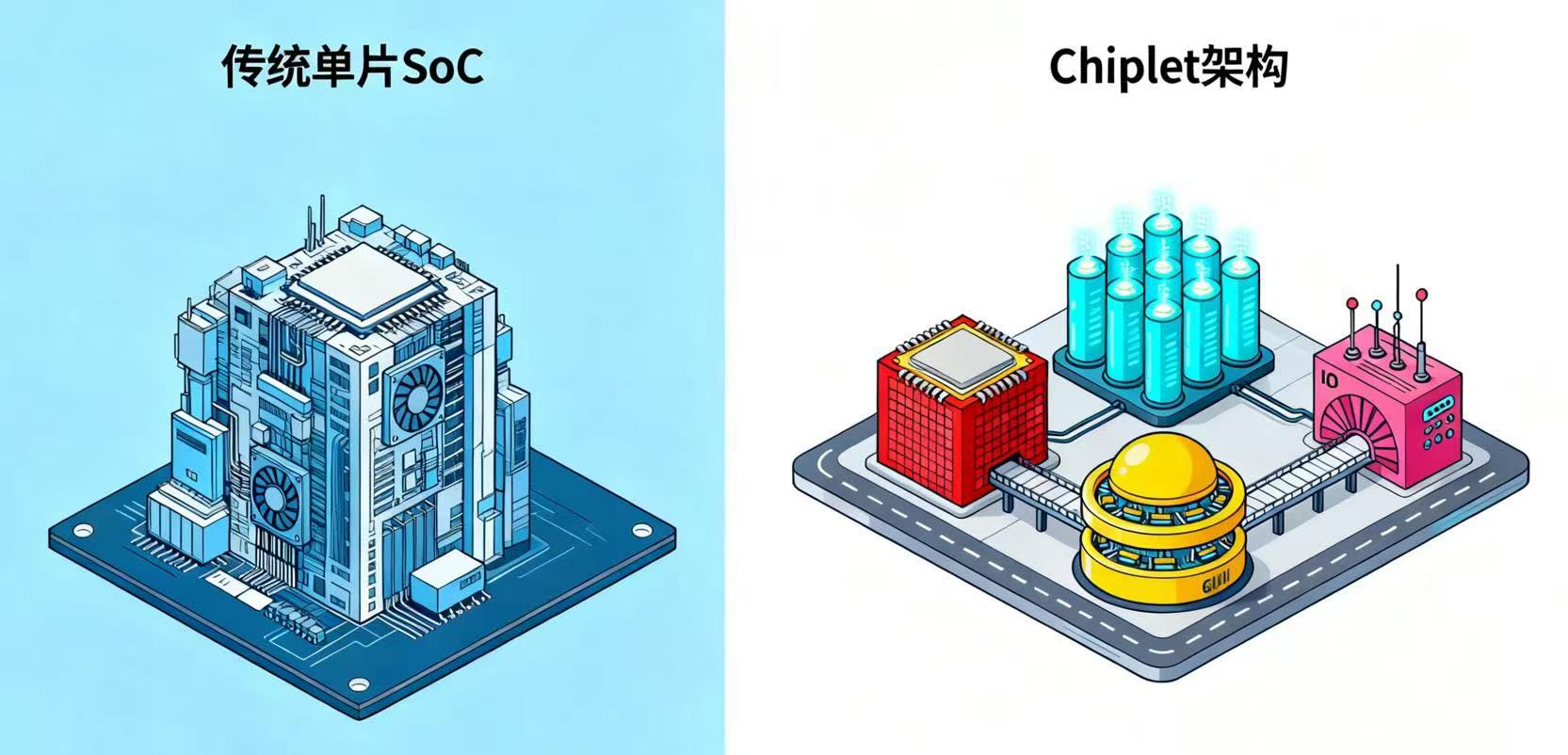
Chiplet Definition: A traditional monolithic SoC is split into multiple independent functional small chips (chiplets) (e.g., CPU/GPU/memory/I/O chiplets), manufactured using different process nodes, and then densely interconnected through advanced packaging to form a complete system-on-chip.
• Core Value (Four Breakthroughs):
1. Yield Leap: Small chiplets (<200mm²) achieve="" while="" large="" socs="">800mm²) have<50% yield, reducing costs by 50%-70%.<!--200mm²)-->
2. Process Freedom: Compute chiplets use 3/5nm, I/O/analog use 12/28nm, memory uses mature nodes – select the optimal process for each function to achieve the best performance-cost ratio.
3. Module Reuse: The same chiplet (e.g., Zen4 CPU) can be paired with different I/O/memory chiplets to quickly derive multiple models, shortening development cycles.
4. Bandwidth Breakthrough: Interconnect bandwidth between chiplets reaches TB/s level, far exceeding traditional PCB GB/s level, meeting the high bandwidth demands of AI.
2.2 Main Technology Types (by Integration Dimension)
1) 2D MCM (Multi-Chip Module, First-Generation Chiplet)
• Structure: Multiple chiplets are placed side by side on a common substrate (PCB/ceramic), interconnected via wire bonding or flip-chip.
• Characteristics: Low cost, low bandwidth (20-50GB/s), high latency – suitable for low-end servers/consumer electronics (e.g., early AMD EPYC Naples).
2) 2.5D Packaging (Silicon Interposer, Current Mainstream)
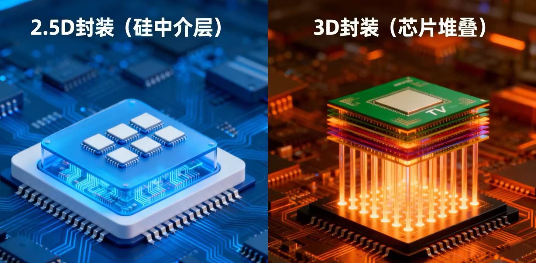
• Structure: Chiplets are attached to a silicon interposer (with TSVs – Through-Silicon Vias), which provides high-density routing interconnection before connecting to the substrate.
• Characteristics: High bandwidth (1.2TB/s), low latency, good heat dissipation – suitable for GPU/FPGA/AI chips (TSMC CoWoS, AMD Instinct MI100).
3) 3D Packaging (Vertical Stacking, Next-Generation Core)
• Structure: Chiplets are stacked vertically (logic + memory / logic + logic), interconnected directly via TSV/hybrid bonding with vertical signal transmission.
• Characteristics: Highest bandwidth, lowest latency, smallest footprint – challenges include thermal dissipation and yield (Intel Foveros, Samsung X-Cube, AMD 3D V-Cache).
4) FOWLP/FO-PLP (Fan-Out Packaging, Low Cost, High Performance)
• Structure: No interposer; chiplets are directly embedded in redistribution layers (RDL) with fan-out routing interconnection – lower cost than 2.5D.
• Characteristics: Balances performance and cost – suitable for mid-to-high-end chiplets (e.g., Apple A-series, some AI inference chips).
2.3 Evolution Path: From Discrete to Converged, from Homogeneous to Heterogeneous
Stage 1: Infancy (1980s-2010s) – 2D MCM
• Technology: Multi-chip substrate integration, sparse interconnection, low bandwidth.
• Representative: Early server CPUs, mobile phone baseband chips.
Stage 2: Growth (2010s-2020s) – 2.5D + Chiplet Concept Explosion
• Technology: Silicon interposer matures, Chiplet architecture proposed, AMD first to commercialize (Zen2/Zen3).
• Representative: AMD EPYC, NVIDIA A100, TSMC CoWoS.
Stage 3: Maturity (2020s-2030s) – 3D + Heterogeneous Integration + Standardization
• Technology: Hybrid bonding becomes widespread, pitch shrinks to<1μm; interface standards like UCIe; heterogeneous integration of logic/memory/optics.
• Representative: AMD Zen4 (3D V-Cache), Intel Foveros, Apple M-series Ultra.
Stage 4: Future (2030s+) – Optoelectronic Integration + Material Innovation
• Technology: Optical interconnects replace some electrical interconnects, bandwidth exceeds 10TB/s; heterogeneous integration of new materials such as silicon + GaN/SiC.
III. Heterogeneous Integration Technology: System-Level Fusion Across Processes/Materials/Functions
3.1 Technical Logic: Breaking Through Single-Chip Boundaries, Multi-Dimensional Heterogeneous Collaboration
Heterogeneous Integration Definition: The integration of chips/devices of different process nodes, different material systems, and different functional types (e.g., logic + memory, silicon + photonics, CMOS + GaN) within the same package, achieving "1+1>2" system performance.
• Three Heterogeneous Dimensions:
1. Process Heterogeneity: 5nm logic + 28nm analog + 14nm memory – avoids the high cost of advanced process across the board.
2. Functional Heterogeneity: CPU + GPU + HBM + AI accelerator + optical module – optimizes computing power, bandwidth, and energy efficiency.
3. Material Heterogeneity: Silicon (CMOS) + Gallium Nitride (power) + Indium Phosphide (photonics) – breaks through silicon-based physical limits.
3.2 Core Technology System (Key Enablers of Heterogeneous Integration)
1) High-Density Interconnect Technology
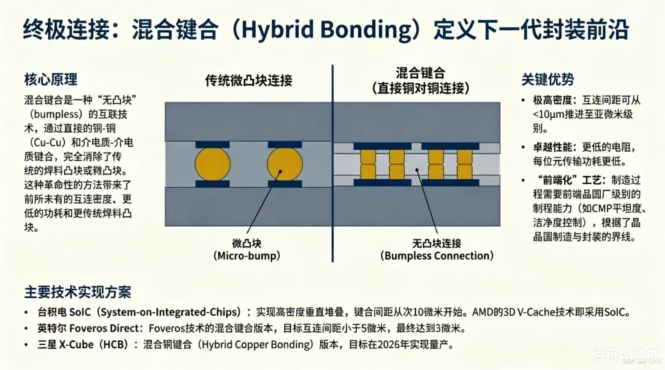
• Micro Bumps: Pitch 50-100μm, mainstream for 2.5D, TB/s bandwidth.
• Hybrid Bonding: Pitch<1μm, bumpless, direct copper-copper bonding, core for 3D, highest bandwidth and lowest latency (TSMC SoIC, Intel Foveros Direct).
2) Interposer/Bridge Technology
• Silicon Interposer: Core for 2.5D, high-density TSV/RDL, interconnect density 10^4 I/O/mm².
• RDL Interposer (Si-less): Used in FOWLP, lower cost, interconnect density 10^3 I/O/mm².
• EMIB (Embedded Multi-Die Interconnect Bridge): Intel patent, localized high-density interconnect, lower cost than full silicon interposer.
3) 3D Stacking and Thermal Management
• TSV (Through-Silicon Via): Vertical interconnect, shortens signal path, essential for 3D.
• Thermal Management: Microfluidic cooling, thermal interface material optimization, partitioned chiplet heat dissipation – addressing the overheating bottleneck in stacking.
4) Interface Standardization (Key to Ecosystem)
• UCIe (Universal Chiplet Interconnect Express): Released in 2022, jointly developed by AMD, Intel, TSMC, NVIDIA – a high-speed interconnect standard between chiplets, 1.5TB/s bandwidth, supporting cross-vendor interoperability.
• Others: PCIe 6.0, CXL 3.0 (chip-memory interconnect), BoW (bandwidth-optimized interface).
3.3 Evolution Path: From Chip-Level to Material-Level, from Electrical to Optical Interconnect
1) Chip-Level Heterogeneous Integration (2020s, Current Mainstream)
• Integration: Chiplets of different functions/process nodes (e.g., CPU+HBM, GPU+AI accelerator).
• Technology: 2.5D + micro bumps, early adoption of UCIe.
• Representative: AMD MI300 (5nm GPU + 6nm I/O + 4nm logic), NVIDIA Grace Hopper.
2) Device-Level Heterogeneous Integration (2025-2030, Early Commercialization)
• Integration: Different devices within the same chip (e.g., silicon CMOS + GaN transistors, silicon photonics + logic).
• Technology: 3D hybrid bonding, pitch<500nm, optimized thermal management.
• Applications: AI chips, 5G/6G RF, autonomous driving domain controllers.
3) Material-Level Heterogeneous Integration (2030s+, Future Core)
• Integration: Different semiconductor materials (silicon + silicon carbide + indium phosphide + 2D materials).
• Technology: Breakthroughs in heteroepitaxy and bonding technologies; optical interconnects replace electrical interconnects.
• Applications: Ultra-high-speed optical computing, quantum computing interfaces, extreme-environment electronics.
IV. Relationship Between Chiplet and Heterogeneous Integration: Complementary, Deeply Integrated
• Chiplet is the core enabler of heterogeneous integration: The modular architecture of chiplets naturally supports heterogeneous combinations of different chiplets, making it the most mature implementation of heterogeneous integration.
• Heterogeneous integration extends the value of Chiplets: Early chiplets were primarily homogeneous (e.g., multiple CPU cores); heterogeneous integration (logic + memory + photonics) further unlocks the performance potential of chiplets.
• Common goal: Break through Moore's Law limitations, replacing "transistor scaling" with "system integration" to achieve exponential improvements in computing power, bandwidth, and energy efficiency.
V. Industry Challenges and Breakthrough Directions
5.1 Core Challenges
1. Interconnect Bottleneck: Bandwidth demand exceeds 10TB/s; electrical interconnects approach physical limits, with prominent trade-offs between latency and heat dissipation.
2. Lack of Standardization: UCIe ecosystem needs further development; cross-vendor chiplet interoperability remains difficult; lack of uniform interface, testing, and packaging standards.
3. Cost and Yield: 2.5D/3D packaging costs are high (accounting for 30%-50% of total chip cost); yield control for stacking is challenging.
4. Design and Test Complexity: Multi-chiplet co-design, signal integrity simulation, cross-process testing and validation are highly challenging.
5.2 Breakthrough Directions
1. Technological Breakthroughs: Widespread adoption of hybrid bonding, integration of optical interconnects, development of low-cost interposers (e.g., glass interposers).
2. Ecosystem Development: Advancement of UCIe/CXL standardization, establishment of KGD (Known Good Die) chiplet libraries to lower design barriers.
3. Cost Optimization: FOWLP/FO-PLP replacing some 2.5D applications, reuse of mature processes, scaling production for cost reduction.
4. Collaborative Innovation: Collaboration across the entire design-manufacturing-packaging-testing chain; development of dedicated EDA tools and testing solutions for chiplets.
VI. Future Outlook: Advanced Packaging Defines Next-Generation Chips
• Short Term (2025-2027): 2.5D + Chiplet mainstream; UCIe ecosystem matures; 3D hybrid bonding sees small-scale commercial use; AI/data center chips lead adoption.
• Medium Term (2028-2030): 3D heterogeneous integration becomes standard for high-end chips; logic + memory + photonics converge; optical interconnect technology breakthroughs; costs drop by 50%+.
• Long Term (2030s+): Material-level heterogeneous integration becomes widespread; silicon-based and non-silicon-based materials converge; optical and quantum integration emerges; advanced packaging evolves from "chip packaging" to the core of "system manufacturing."
Shanghai Liyuan Micro Semiconductor Co., Ltd. is a professional SiP system-level packaging solution development platform. For many years, we have provided customers with one-stop services and solutions including ASIC chip design,
SiP packaging design and simulation, wafer procurement for internal SiP use, packaging production, system-level testing, reliability and failure analysis.
Our company offers free SiP/Chiplet design consulting and services to all customers. We are dedicated to helping customers achieve design goals such as small form factor, low power consumption, and low cost.
If interested, please feel free to contact us at 13817180836 (WeChat ID same as phone number).