Chip World's "LEGO Magic": A Comprehensive Introduction to Chiplet Packaging Technology
Have you ever wondered how a fingernail-sized chip in your phone or computer can hold billions of transistors? In the past, making a chip was like carving a whole piece of jade – one small mistake and it was scrapped;
Now, with Chiplet technology, it's like playing with LEGO bricks – breaking a large chip into small modules and then precisely assembling them, making it both powerful and cost-effective! Today, let's help you understand this black technology of the post-Moore era.
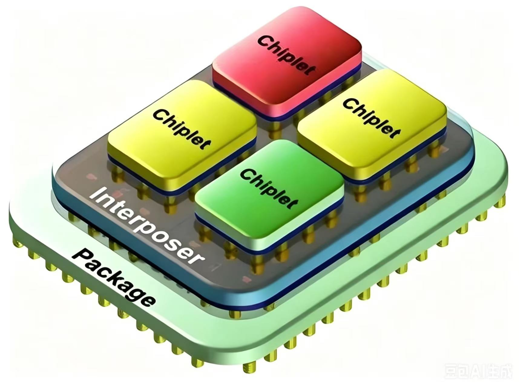
I. What is Chiplet? Breaking a "Behemoth" into "Little Experts"
A traditional chip (SoC) is like a whole family living in one large flat: compute cores, memory, interfaces, signal processing – all crammed onto the same silicon die, manufactured in one go using the most advanced 3nm or 5nm processes.
But large chips have many problems:
• The larger the area, the more prone to manufacturing defects – low yield, skyrocketing costs
• All functions are forced to use the same process – wasteful and mismatched (e.g., I/O interfaces don't need cutting-edge nodes)
• Design difficulty explodes, development cycles get longer and longer
Chiplet takes a different approach: divide and conquer
Break a large system into multiple function-specific small chips (chiplets):
• Some specialize in high-speed computing (CPU/GPU chiplets)
• Some are responsible for data storage (HBM memory chiplets)
• Some handle input/output (I/O interface chiplets)
• Some process AI operations (NPU chiplets)
Then, using advanced packaging technology, they are "glued" together to form a complete super-chip – just like LEGO bricks, where different parts can be assembled into any shape!
II. How are they assembled? 3 Packaging "Black Magics"
For small chiplets to work together perfectly, three packaging techniques – 2D, 2.5D, and 3D – are used, with connection density and difficulty increasing at each level.
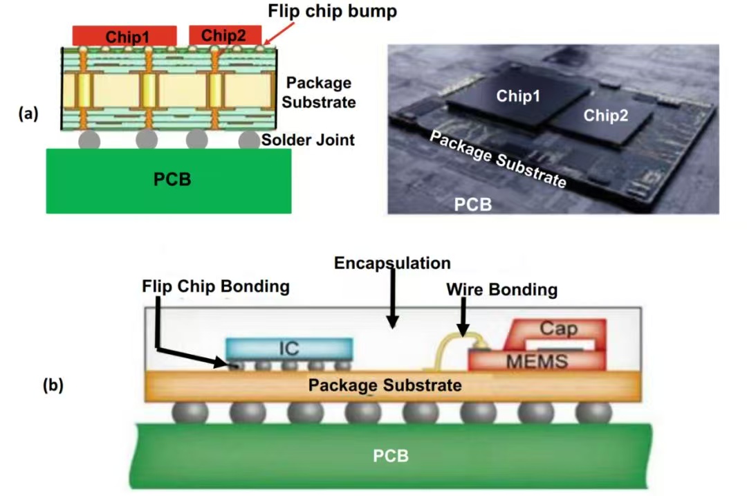
1. 2D Packaging: "Buddies" Sitting Side by Side
The most basic approach: all chiplets are laid flat on the same packaging substrate and connected using ordinary traces.
• Advantages: Mature technology, low cost, good heat dissipation
• Disadvantages: Long connection distances, limited bandwidth, large footprint
• Suitable for: Low-end chips, simple functional combinations
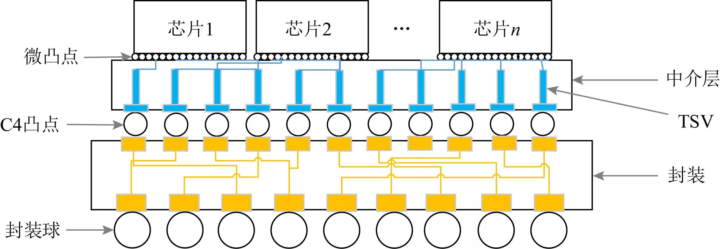
2. 2.5D Packaging: A Large Flat with "Underground Passages"
The mainstream solution for today's high-end chips (AI, GPUs)!
A silicon interposer is added between the chiplets and the substrate, containing countless ultra-dense traces and Through-Silicon Vias (TSVs).
• Analogy: Several buildings built on the same "underground foundation," connected via high-speed underground passages
• Advantages: Extremely short connections, ultra-large bandwidth, ultra-low latency, stable signals
• Disadvantages: Relatively high cost, complex process
• Representatives: AMD Ryzen, NVIDIA AI chips, TSMC CoWoS
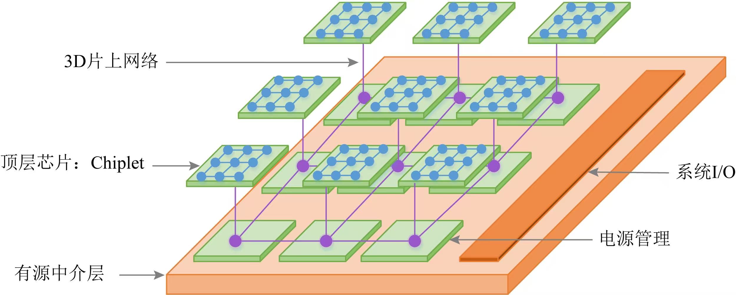
3. 3D Packaging: A Stacked "Skyscraper"
The most radical black technology: stacking chiplets vertically, layering them like building a skyscraper, directly connecting them vertically using TSVs.
• Advantages: Smallest footprint, highest bandwidth, lowest power consumption, strongest performance
• Disadvantages: Extremely difficult process, major heat dissipation challenges, highest cost
• Future: Next-generation high-performance CPUs, supercomputers, HBM high-bandwidth memory
III. What makes Chiplet so appealing? 4 Core Advantages
1. Cost-effective! Yield skyrockets, costs plummet
Large chip yield may be only 40%-50% – one defect and the whole thing is scrapped;
After being broken into small chiplets, yield easily exceeds 90% – if one is bad, just replace that one, no need to discard the whole batch – manufacturing costs are cut in half!
2. Freely mix and match! The joy of heterogeneous integration
Different chiplets can be manufactured using different processes:
• Compute cores: Use cutting-edge 3nm process for maximum performance
• I/O/Memory: Use mature 22nm process to save cost
• Even chiplets of different materials and from different vendors can be assembled together – achieving the perfect balance between performance and cost
3. Flexible and fast! Customize like building with blocks
No need to design the entire chip from scratch – just combine existing chiplets:
• Need more computing power? Add more compute chiplets
• Need more memory? Add HBM memory chiplets
• Product iteration speeds up, time-to-market cut in half
4. Extending Moore's Law! Breaking through physical limits
Transistors are approaching atomic sizes, and traditional processes are reaching their end.
Instead of forcing process node scaling, Chiplet improves performance through "stacking and assembling" – giving Moore's Law a new lease on life!
IV. Challenges and Future: The "Block Ecosystem" Still Under Refinement
Even the best technology has its shortcomings:
• Communication difficulties: Inter-chiplet interconnection requires ultra-high-speed, low-latency standards (e.g., UCIe)
• Heat dissipation pressure: Dense stacking makes heat difficult to dissipate
• Ecosystem not yet mature: Interface, design, and testing standards are still being unified
But it is already recognized by the semiconductor industry as the future: from AMD, Intel, TSMC to domestic chip manufacturers – all are betting heavily on it.
Future smartphones, AI servers, and autonomous driving chips will almost all be super-brains assembled from Chiplet blocks!
In short: Chiplet is the modular revolution in the chip world, turning complexity into simplicity, turning expensive into affordable, turning limits into infinity.
Next time you see "Chiplet," don't think it's too profound – it's the LEGO-like black technology that makes your phone faster and your computer stronger!
Shanghai Liyuan Micro Semiconductor Co., Ltd. is a professional SiP system-level packaging solution development platform. For many years, we have provided customers with one-stop services and solutions including ASIC chip design, SiP packaging design and simulation, wafer procurement for internal SiP use,
packaging production, system-level testing, reliability and failure analysis. Our company offers free SiP/Chiplet design consulting and services to all customers,
and is dedicated to helping customers achieve design goals such as small form factor, low power consumption, and low cost. If interested, please feel free to contact us at 13817180836 (WeChat ID same as phone number).