CSPT2026 Preview | Advanced Packaging: Not Incremental, But Revolutionary!
As the death knell of Moore's Law grows louder and transistor dimensions approach their physical limits, everyone believed the growth of chip performance was about to hit the brakes.
But at CSPT (China Semiconductor Packaging & Testing Expo) 2026, a disruptive revolution is erupting—advanced packaging is reshaping the entire semiconductor industry landscape with overwhelming force.
This is not mere incremental patching of the past; it is a comprehensive reconstruction from fundamental logic, materials, and architecture to production capacity!
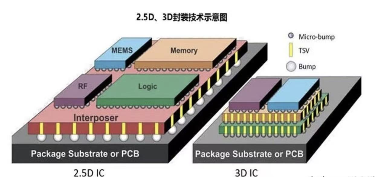
I. From "Round" to "Square": An Industry Earthquake Triggered by Shape
Can you believe it? The round wafer that has dominated the semiconductor industry for over half a century is being completely abandoned.
TSMC's CoPoS (Chip-on-Panel-on-Substrate) technology, unveiled on the eve of CSPT2026, is the very fuse of this revolution. Its core essence can be summed up in four words: turning round into square.
• Past (Round): 12-inch round wafers, massive edge waste after dicing, material utilization rate of only 67%.
• Present (Square): 310×310mm ultra-large square glass panels, seamless splicing, utilization rate soaring directly to 90%+.
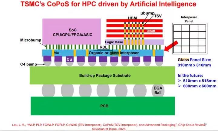
Don't underestimate this change in shape! It brings an industry earthquake of doubled production capacity and a 30% cost plunge.
The high-end packaging capacity that AI chip giants were fiercely scrambling for is suddenly liberated overnight. This is not optimization—this is revolution!
II. Materials Revolution: Glass Replaces Silicon, the "Invisible Backbone" of AI Computing Power
If shape is the outward manifestation, then the replacement of materials is the hardest-core fundamental revolution in advanced packaging.
Traditional silicon interposers (CoWoS) have become inadequate in the AI era: excessive heat generation, susceptibility to warping, and high cost. The emergence of glass substrates (TGV) has perfectly solved all these pain points:
• Speed Revolution: 3.5x increase in signal transmission rate
• Power Efficiency Revolution: 30% reduction in overall power consumption
• Volume Revolution: Supports ultra-large 515×510mm dimensions, 4-8 times that of 12-inch wafers
• Cost Revolution: 30% direct reduction in overall packaging cost
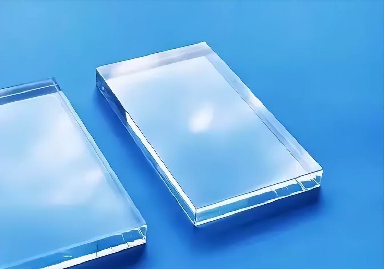
From silicon to glass, this is the Cambrian explosion of packaging materials. At CSPT2026, glass substrates have become the focal point of the entire event, with giants like Intel and TSMC collectively placing their bets, marking its formal transition from concept to large-scale commercialization.
III. Chiplet + 3D Stacking: The "Lego Building Blocks" Era of Chips
If a traditional chip is likened to a sculpture carved from a single block of marble, then Chiplet + 3D stacking technology turns chips into Lego building blocks.
• Break the Whole into Parts: Split a super-large chip (SoC) into multiple "chiplets" such as CPU, GPU, and memory.
• Heterogeneous Integration: Chiplets with different processes and functions can be freely combined like building blocks.
• Vertical Stacking: Transforming from "laying flat" to "building high-rises," signal paths are shortened by 100 times, bandwidth soars while power consumption plummets.
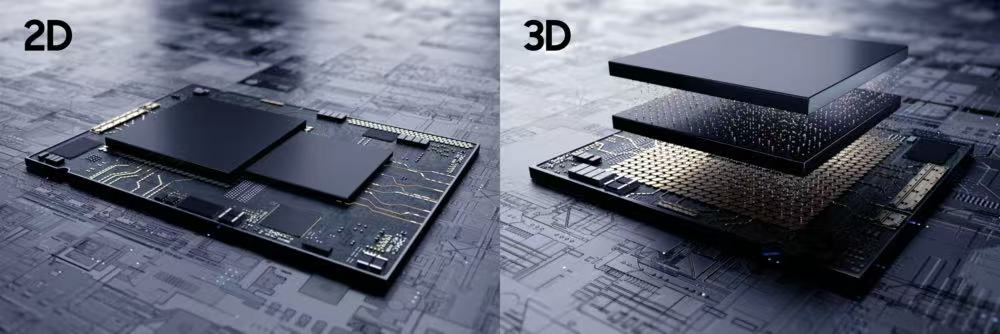
At the CSPT2026 venue, you can witness the most cutting-edge Hybrid Bonding technology:
• Traditional: Connection via solder bumps (pitch >10μm)
• Present: Direct copper-to-copper bonding, bumpless, seamless interconnection (pitch ≤1μm)
• Result: 10x increase in interconnect density, performance rivaling monolithic SoCs
IV. Why Is This "Revolutionary" Rather Than "Evolutionary"?
Many will ask, isn't packaging just the "clothing" of the chip? It has been upgrading all along, so why is it different this time?
Because in the past, packaging played a supporting role; today, advanced packaging has risen to become the lead.
1. Value Center Shift: Packaging has transformed from a "backend process" into the core bottleneck determining AI chip performance. Performance improvement no longer relies on process nodes—70% now depends on packaging.
2. Industry Rules Rewritten: No longer about "process-node supremacy" (7nm, 5nm). Chiplets from trailing nodes, through advanced packaging, can also deliver a winning combination.
3. Capacity and Cost Disruption: Technologies like CoPoS double capacity and slash costs by half, directly addressing the urgent AI computing power shortage.
V. CSPT2026: Witnessing the Rise of China's "Core" Strength
In this global packaging revolution sweeping the world, China's strength has never been absent.
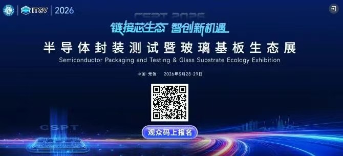
As China's premier exhibition for the packaging and testing industry, CSPT2026 brings together domestic leaders such as JCET, Tongfu Microelectronics, and SJ Semiconductor.
The cutting-edge technologies they bring—2.5D/3D packaging, glass substrates, hybrid bonding, and more—are achieving a leap from "following" to "running in parallel," and even leading in certain areas.
Conclusion: In the Post-Moore Era, Packaging Is the Future
Looking back from the vantage point of CSPT2026, we see clearly:
Advanced packaging is not the dessert—it is the main course; not a patch, but a reconstruction.
It breaks the century-old shackles of the round wafer with square glass;
It reconstructs chip design philosophy with Chiplet building blocks;
It unblocks the meridians of AI computing power with 3D stacking.
2026 marks the inaugural year of advanced packaging's transition from the laboratory to large-scale mass production. This revolution has only just begun, and it will profoundly influence every smartphone, every server, and every AI interaction in the decade to come.
Packaging is dead, long live packaging—revolutionary advanced packaging is the ultimate answer in the post-Moore era!
Shanghai Liyuan Micro Semiconductor Co., Ltd. is a professional SiP system-in-package solution development platform. For many years, we have provided customers with one-stop services and solutions including ASIC chip design, SiP packaging design and simulation, SiP internal wafer procurement, packaging production,
system-level testing, reliability and failure analysis, and more. Our company offers free SiP/Chiplet design consultation and services to all customers, dedicated to helping clients achieve design goals such as small form factor, low power consumption,
and low cost. If interested, please feel free to contact us at +86 13817180836 (same number for WeChat).