2025 China Advanced Packaging Industry Market Prospect Forecast Research Report
As chip manufacturing processes become increasingly challenging and Moore's Law slows down, advanced packaging has emerged as the "black technology" that makes chips more powerful and more affordable.
In 2025, China's market for this technology is ushering in a hundred-billion-yuan explosive growth phase. Below, we break down the current landscape, scale, technology, competitive dynamics, and prospects in simple, accessible terms.
I. What Is Advanced Packaging? A One-Sentence Primer
Traditional packaging merely "dresses" the chip; advanced packaging integrates multiple chips at high density like building blocks (2.5D/3D stacking, Chiplet technology),
delivering a massive boost in performance and a dramatic reduction in cost—making it the core track of the "post-Moore era."
II. 2025 Market Scale: China's Growth Rate Leads the World
• Global: The advanced packaging market in 2025 is approximately USD 571 billion, accounting for over 51% of the total packaging and testing market for the first time, becoming the absolute mainstream.
• China: The scale in 2025 exceeds RMB 1,100 billion (approx. RMB 85.2–110 billion), with a CAGR of 18.7% from 2020 to 2025, far outpacing the global rate.
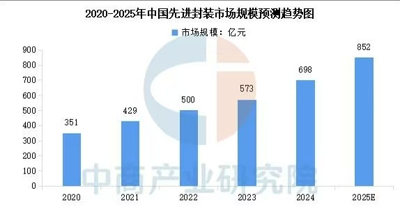
III. Core Growth Drivers: AI and Domestic Substitution as Twin Engines
1. AI Explosion
AI chips (such as those for large language models, H100-class) demand ultra-high bandwidth and ultra-low latency—requirements only 2.5D/3D + Chiplet can satisfy. AI-related packaging is growing at 46% per year, the industry's fastest engine.
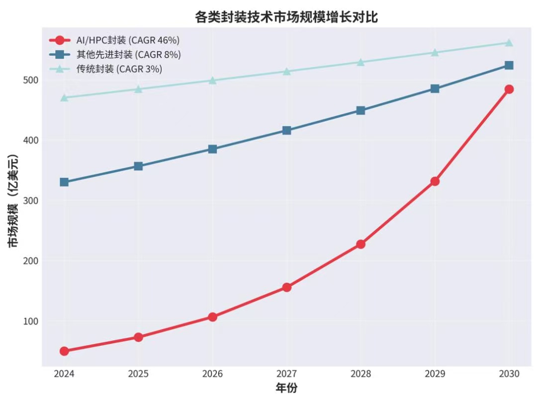
2. Accelerating Domestic Substitution
China is the world's largest chip consumer, yet high-end packaging has long depended on external sources. In 2025, the domestic substitution rate will exceed 50%, with supportive policies and major national funds continuously increasing investment, enabling local enterprises to rapidly fill the gap.
IV. Mainstream Technologies: Who Dominates in 2025?
• Chiplet: Accounts for 38.2% of the China market. Dismantles a large chip into small modules to be "assembled like building blocks," cutting costs by 40% and boosting efficiency by 60%.
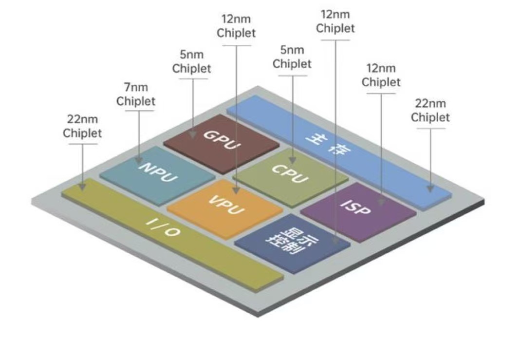
• 2.5D/3D Packaging: Accounts for 26.5%. Utilizes silicon interposers + TSV vias to achieve vertical/high-density interconnection—a standard configuration for AI chips.
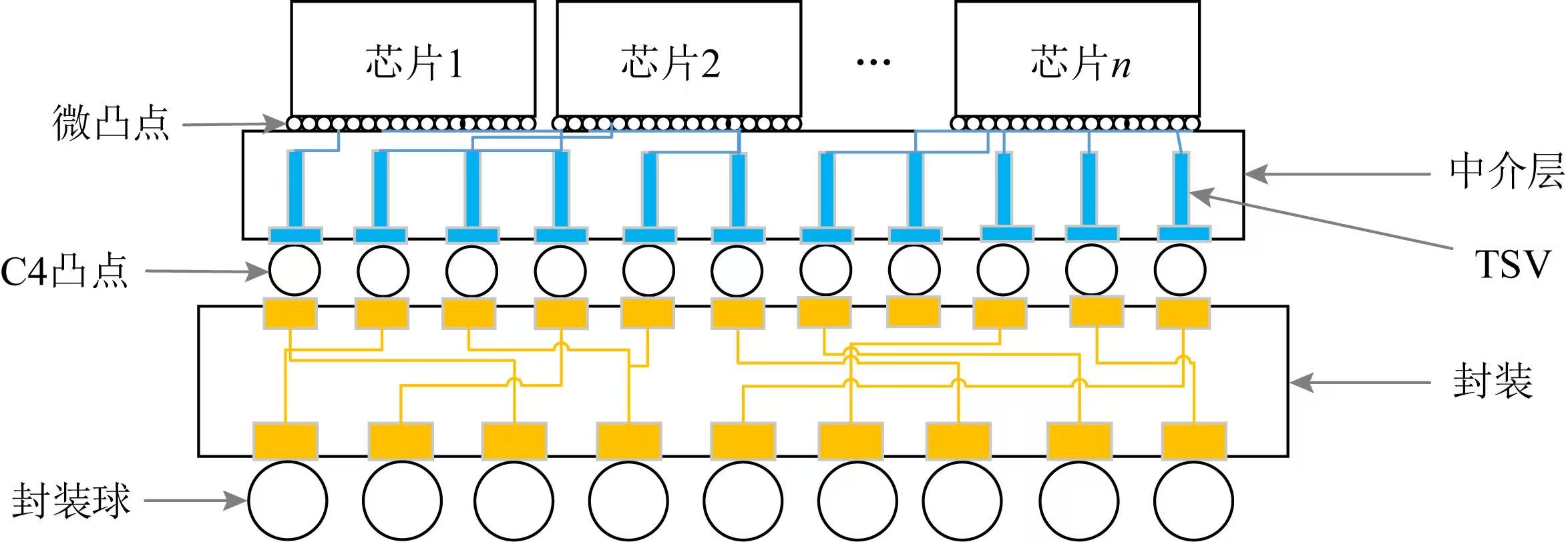
• Flip Chip (FC), Fan-Out (FO), SiP: Mature and stable, covering smartphones, IoT, and automotive electronics.
V. China's Industry Landscape: Top Three Lead, Yangtze River Delta as the Core
• Domestic Big Three: JCET, Tongfu Microelectronics, and Huatian Technology collectively hold 77% of the domestic advanced packaging market and rank among the global top ten.
• Industry Cluster: The Yangtze River Delta (Jiangsu + Shanghai + Zhejiang) accounts for 68% of national capacity—China's packaging "heart."
• Gap and Opportunity: A 5-8 year gap still remains in high-end 3D and hybrid bonding, but breakthroughs in 2.5D/Chiplet mass production have been achieved. The gap is precisely the opportunity.
VI. Three Key Trends for 2025
1. From "Supporting Role" to "Lead Role": Packaging is no longer a back-end process but the core of computing power competition.
2. Chiplet + 2.5D Become Mainstream: Together accounting for over 64% of the China market, they are mandatory for high-end AI chips.
3. Capacity Shortage, Price Hikes Continue: High-end 2.5D/3D supply falls short of demand; local expansion accelerates, with the domestic substitution rate continuing to jump.
VII. Summary: 2025 Marks the "Golden Inflection Point" for China's Advanced Packaging
• Market: Hundred-billion scale, high growth, driven by the twin engines of AI and domestic substitution.
• Technology: Chiplet + 2.5D dominates, with 3D rapidly catching up.
• Landscape: The local "Big Three" are rising, leaving immense space for high-end substitution.
• Prospect: The next five years remain a golden development period, representing one of the most certain tracks for semiconductor domestic substitution.
Shanghai Liyuan Micro Semiconductor Co., Ltd. is a professional SiP system-in-package solution development platform. For many years, we have provided customers with one-stop services and solutions, including ASIC chip design, SiP packaging design and simulation,
SiP internal wafer procurement, packaging production, system-level testing, reliability and failure analysis, and more. Our company offers free SiP/Chiplet design consultation and services to all customers,
dedicated to helping clients achieve design goals such as small form factor, low power consumption, and low cost. If interested, please feel free to contact us at +86 13817180836 (same number for WeChat).