3D-IC's Three-Layer Revolution: From Transistors to Systems, Turning Chips Into "High-Rise Buildings"
As planar chips approach their performance limits, 3D-IC is propelling integrated circuits out of the two-dimensional plane, mining vertical space for computing power, density, and efficiency!
From individual transistors "standing up," to transistors stacked vertically, to entire chip clusters integrated like high-rise buildings—these three layers of 3D-ization are reshaping the future of chips.
Layer 1: Transistor Structure 3D-ization—From "Laying Flat" to "Standing Up"
The earliest chip transistors were Planar FETs, like small switches laid flat on a silicon wafer in a 2D planar arrangement. But as dimensions continued shrinking, leakage and power consumption problems became increasingly severe.
Thus, FinFET emerged! It shaped the transistor channel into a "fin," standing upright from the plane—equivalent to adding a three-dimensional wall to the switch, tightly controlling current flow and dramatically reducing leakage.
The later GAAFET (Gate-All-Around FET) is even more extreme, with the gate fully surrounding the channel like a "ring," achieving a more perfect 3D structure and further elevating performance.
Simply put: This layer is the 3D-ization of individual transistors, transforming the "small switch" from lying flat to standing upright—the fundamental first step of 3D-IC.
Layer 2: Transistor 3D Integration—Stacking the "Switches" Top and Bottom
FinFET and GAAFET only make individual transistors three-dimensional but have not yet achieved "stacking." In contrast, CFET (Complementary FET) targets "vertical transistor stacking"
—directly stacking N-type and P-type transistors one on top of the other like building blocks, connected by nanoscale channels.
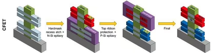
This step is transistor 3D integration, packing more transistors into a fingernail-sized chip with shorter interconnects, faster signals, and lower power consumption. This technology is still under development, expected to reach commercialization in 8–10 years, and is key to future ultimate performance.
Layer 3: Transistor Group 3D Integration—Chip "High-Rises," System-Level Upgrade
If the first two layers are "individual room renovations," the third layer is the three-dimensional construction of an entire building—vertically stacking groups of transistors (i.e., chips/chiplets with different functions) through advanced packaging technology to form a complete 3D system.
Familiar examples like HBM (High Bandwidth Memory) and CPU 3D V-Cache stacking are all applications of this technology layer.
It does not obsess over pushing the limits of a single process; instead, it flexibly combines logic chips, memory chips, and chiplets of different process nodes, maximizing system space and sending functional density soaring.
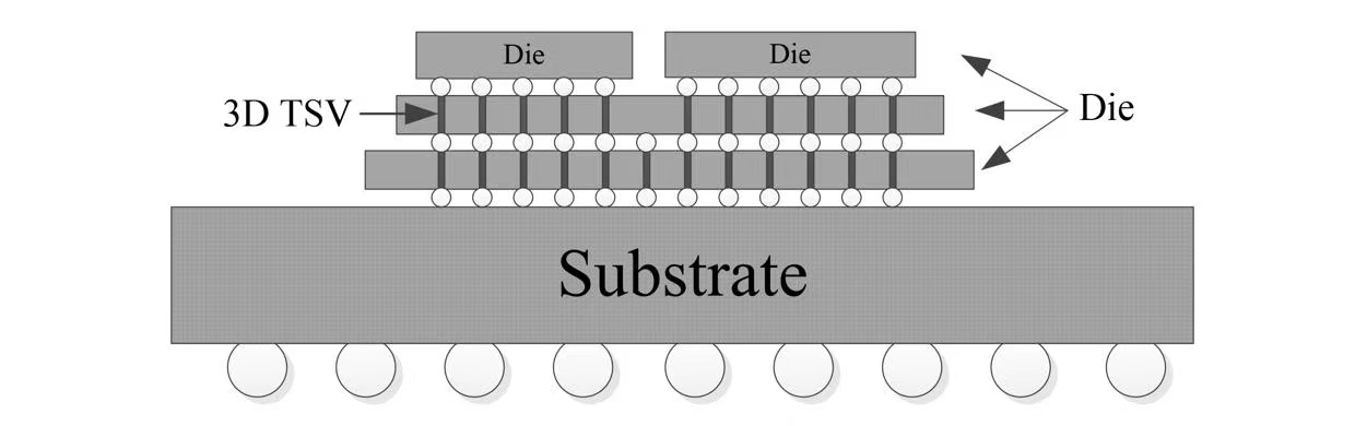
Simply put: This layer is the 3D integration of transistor groups, and it represents the most mainstream form of 3D-IC today, transforming chips from "planar pathways" into "three-dimensional expressway networks."
Three Layers of 3D, United to Break Limits
From transistor structure 3D-ization (FinFET/GAAFET), to transistor 3D integration (CFET), to transistor group 3D integration (advanced packaging)—the three layers progress step by step and complement one another.
Their shared goal is to break the bottleneck of Moore's Law's slowdown, packing more computing power into limited space, making chips run faster, consume less power, and occupy smaller volumes
—whether for smartphones, computers, large AI models, or supercomputers, all will rely on these three layers of 3D technology to unlock greater performance.
Shanghai Liyuan Micro Semiconductor Co., Ltd. is a professional SiP system-in-package solution development platform. For many years, we have provided customers with one-stop services and solutions, including ASIC chip design, SiP packaging design and simulation,
SiP internal wafer procurement, packaging production, system-level testing, reliability and failure analysis, and more. Our company offers free SiP/Chiplet design consultation and services to all customers,
dedicated to helping clients achieve design goals such as small form factor, low power consumption, and low cost. If interested, please feel free to contact us at +86 13817180836 (same number for WeChat).