Advanced Packaging Technology Decoded | Intel: Playing with Chips Like Lego, Breaking Through Performance Limits
As smartphones grow thinner, AI gets smarter, and computers run faster, a key secret hides behind it all—chip packaging technology. If the chip is the "brain," packaging is the "skull + nerves + blood vessels,"
responsible for protection, connectivity, and power delivery. And Intel is the "Lego Master" who has taken this technology to the extreme!
I. Why Pursue Advanced Packaging? Traditional Packaging Is "No Longer Enough"
In the past, chips were "lone wolves": a single silicon die crammed all functions (compute, storage, I/O), speeding up by shrinking process nodes (from 14nm to 7nm to 3nm). But now they've hit a physical ceiling:
• Dimensions have shrunk to the atomic level, causing soaring leakage, heat, and costs;
• A single chip struggles to balance "high performance + low power + multi-functionality";
• The massive data transfer required by AI and supercomputing outpaces traditional packaging speeds.
Thus, the industry shifted its mindset: break the whole into parts, assemble like building blocks! Large chips are dismantled into multiple small "chiplets" (compute, memory, I/O made separately),
then "pieced" together into a whole using advanced packaging—this is heterogeneous integration, and Intel is the frontrunner in this approach.
II. Intel's Packaging "Big Three": EMIB, Foveros, 3D Stacking
1. EMIB: The "High-Speed Underground Tunnel" Between Chips (2.5D Packaging)
EMIB (Embedded Multi-die Interconnect Bridge), mass-produced in 2017, is Intel's "signature skill."
• Principle: Embeds a tiny silicon bridge within the substrate, like an underground tunnel, allowing side-by-side chiplets to engage in direct "high-speed dialogue" without taking detours.
• Advantages:
◦ Lower cost and higher yield than traditional 2.5D (full silicon interposer);
◦ High bandwidth, low latency—AI chips (like Ponte Vecchio) and Xeon CPUs rely on it for acceleration;
◦ Infinitely scalable, supporting ultra-large packages and HBM (High Bandwidth Memory).
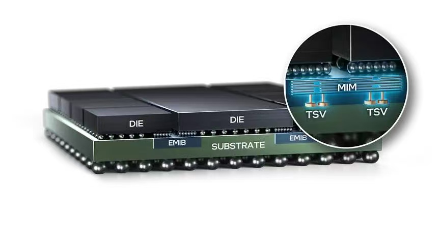
2. Foveros: The "Universal Splicing Baseboard" for Chips (2.5D/3D Packaging)
If EMIB is a "dedicated tunnel," Foveros is a "universal splicing platform," available in three versions—S/R/Direct:
• Foveros-S: Standard silicon interposer, like a large puzzle baseboard, splicing multiple chiplets horizontally—ideal for high-performance scenarios.
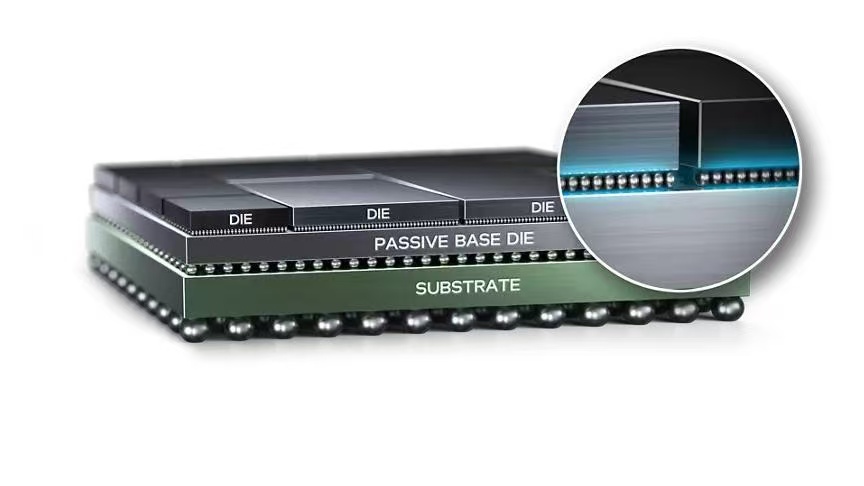
• Foveros-R: Flexible redistribution layer, allowing customizable "wiring" and free adjustment of chiplet positions—lower cost, suitable for mid-range products.
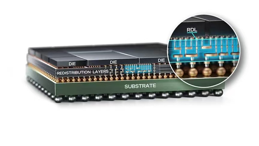
• Foveros Direct: 3D stacking black technology! No solder bumps—direct copper-to-copper "seamless bonding," stacking chips vertically, boosting interconnect density by 10x with near-zero latency.
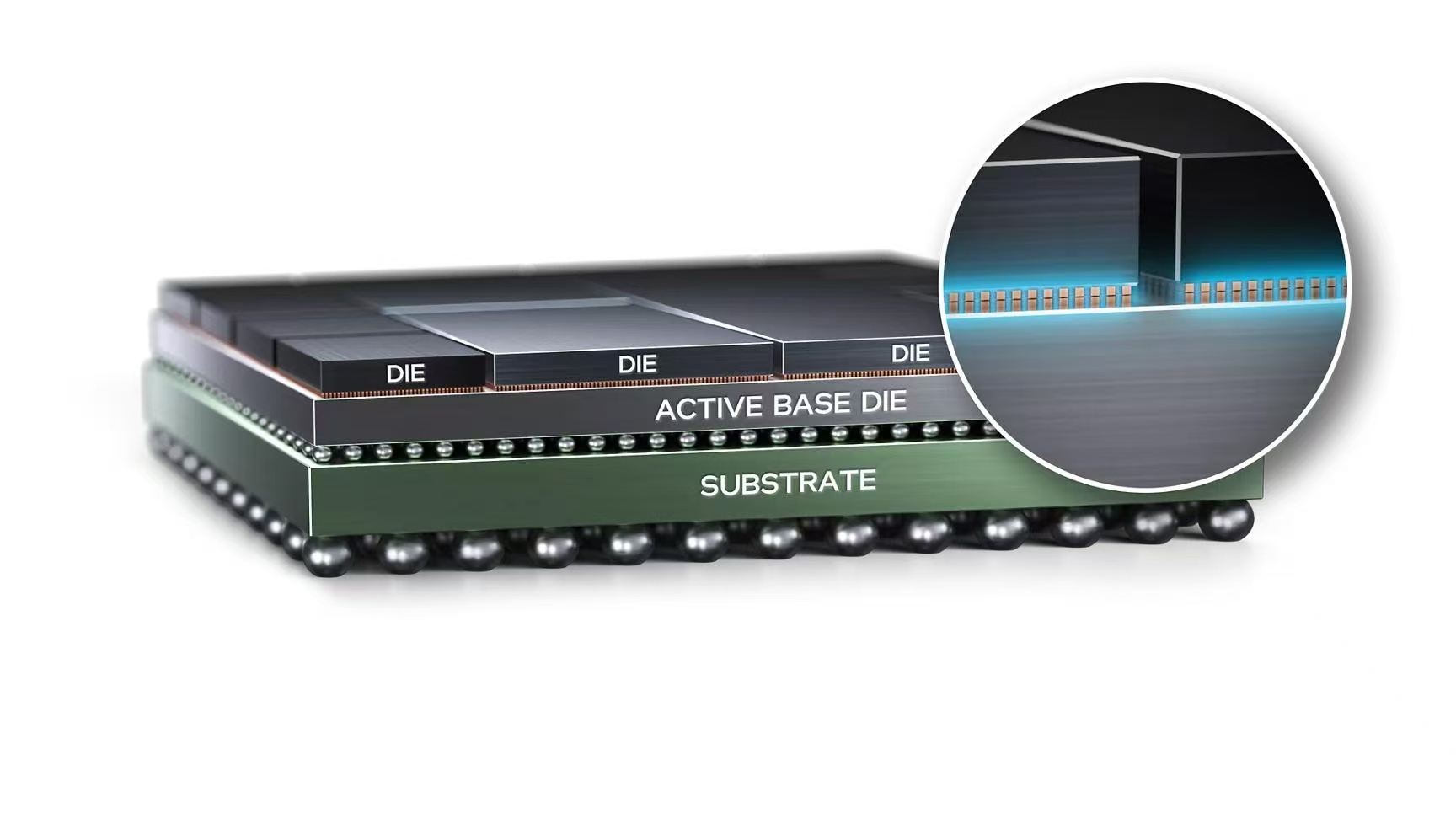
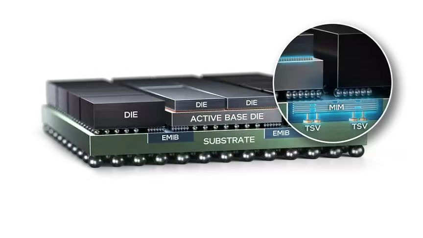
3. 3.5D Packaging: EMIB + Foveros, "Planar + Vertical" Dual Swords Combined
Horizontally connect with EMIB, vertically stack with Foveros, creating a 3.5D super architecture—like building a high-rise: one floor for compute, one for storage, one for I/O, maximizing space utilization and sending performance soaring.
III. Simple Analogies: Understanding How Powerful Intel's Packaging Is
• Traditional Packaging: Individual rooms, messages delivered on foot—slow, prone to traffic jams;
• EMIB (2.5D): High-speed underground tunnels between neighbors—direct, fast, cost-effective;
• Foveros Direct (3D): Floors opened up and down, communicating face-to-face—light-speed transmission;
• 3.5D: A combination of residential blocks + high-rises, connected horizontally and stacked vertically—computing power like a "city power grid" with full coverage.
IV. What Has Intel's Packaging Changed?
1. Breaking Process Node Limits: No need to stubbornly push 3nm/2nm; "building-block assembly" still boosts performance at lower cost;
2. Performance Soars: AI chip bandwidth increases 5x, latency halved—supercomputers and large models run at lightning speed;
3. Flexible Customization: Freely combine chiplets like Lego; customers can build "custom chips" on demand, cutting R&D cycles in half;
4. Industry Benchmark: From EMIB's mass production in 2017 to Foveros Direct's maturity in 2026, Intel has defined advanced packaging standards, propelling the entire industry into the "post-Moore era."
V. Summary: Packaging Is the Core of Future Chips
Today, packaging is no longer a supporting role but a core technology on par with process nodes. With EMIB, Foveros, and 3D stacking, Intel transforms chips from "single components" into "Lego bricks," using "connectivity" to break through physical limits and keep computing power racing ahead.
In the future, whether it's large AI models, autonomous driving, or supercomputers, Intel's advanced packaging will undoubtedly be behind them—strength assembled is true strength.
Shanghai Liyuan Micro Semiconductor Co., Ltd. is a professional SiP system-in-package solution development platform. For many years, we have provided customers with one-stop services and solutions, including ASIC chip design, SiP packaging design and simulation, SiP internal wafer procurement, packaging production, system-level testing,
reliability and failure analysis, and more. Our company offers free SiP/Chiplet design consultation and services to all customers, dedicated to helping clients achieve design goals such as small form factor, low power consumption, and low cost.
If interested, please feel free to contact us at +86 13817180836 (same number for WeChat).