Chip Packaging: The Evolutionary Path from "Protective Shell" to "Performance Engine"
In the semiconductor industry chain, chip design bestows the "soul," wafer fabrication shapes the "body," and packaging is the crucial step that dons a sturdy armor and weaves neural pathways for the chip—it is not only the chip's "protective shell,"
but also the "performance engine" that determines performance, power consumption, and integration density. From micron-scale traditional packaging to heterogeneously integrated advanced technologies, the century-long evolution of packaging is, in essence, a history of innovation chasing "higher density, shorter interconnects, and stronger performance."
I. The Core Value of Packaging: Beyond Just "Protection"
Many mistakenly believe packaging is merely about encasing the chip in a shell, but in reality, it fulfills four core missions, serving as the essential path from "bare die" to "usable device":
• Physical Protection: The core of a chip is a fragile silicon die; packaging isolates it from dust, moisture, static electricity, and mechanical damage, ensuring long-term stability.
• Electrical Interconnection: Via pads, traces, or bumps, the internal circuits of the chip are connected to the external PCB, enabling signal and power transmission.
• Thermal Management: Chips generate heat during operation; packaging (such as the thermal pads in QFN and BGA) is responsible for heat conduction and dissipation, preventing overheating, throttling, or burnout.
• Miniaturization & Standardization: Shrinking chip dimensions and unifying pin specifications to suit automated production and equipment integration.
II. Packaging Evolution: From 2D to 3D, From Single to Integrated
The iteration of packaging technology has always kept pace with rising chip integration levels, passing through five key stages, each breakthrough reshaping the industry landscape.
Stage 1: Through-Hole Mounting Era (Pre-1970) — "Bulky but Simple"
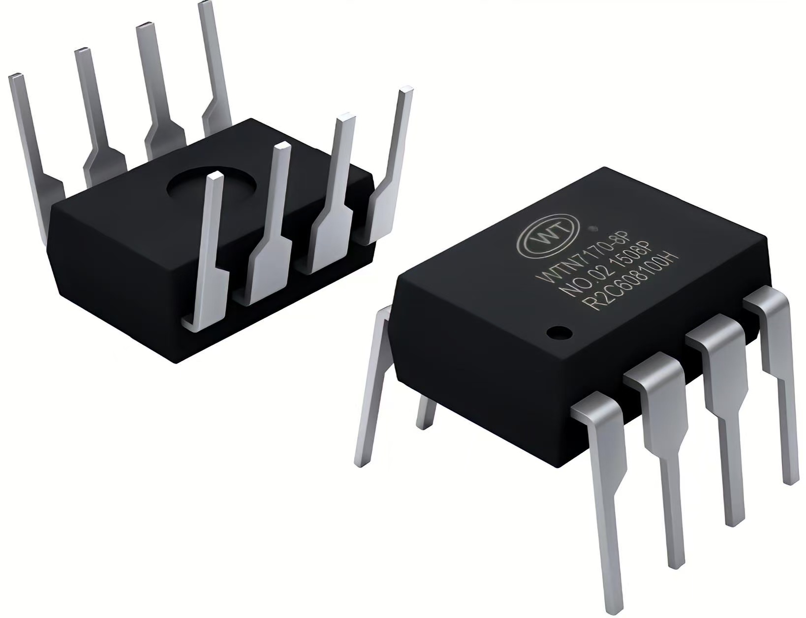
• Representative Technologies: TO packaging (early transistors, 3 pins), DIP (Dual In-line Package) (small-to-medium scale ICs, pins on two sides, 2.54mm pitch).
• Characteristics: Pins required insertion into PCB through-holes for soldering; manual operation was feasible, but density was extremely low, size was large, and traces were long—only suitable for simple circuits (e.g., remote controls, toys).
Stage 2: Surface-Mount Era (1980s) — "Miniaturization, Automation"
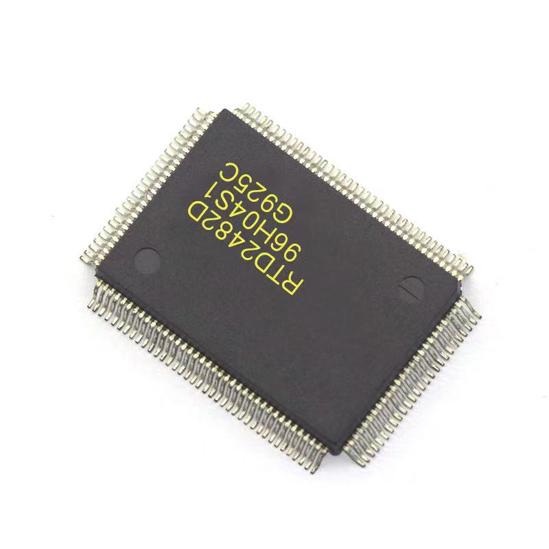
• Representative Technologies: SOP (Small Outline Package), QFP (Quad Flat Package) (pins arranged around four sides, pitch reduced to 0.4mm).
• Characteristics: Pins were soldered flat against the PCB surface, increasing density by 3-5x and enabling automated placement, driving the "lightweighting" of consumer electronics (e.g., early mobile phones, computer motherboards).
Stage 3: Area Array Era (1990s) — "Pins Hidden Underneath, Density Explodes"
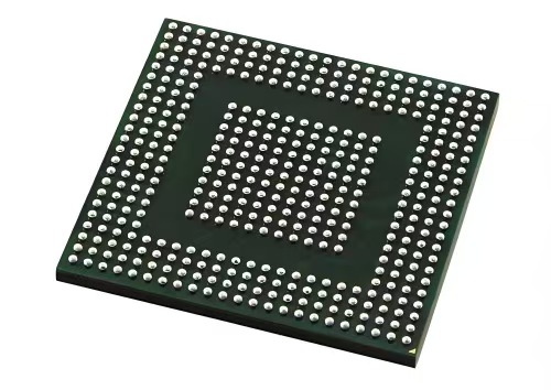
• Representative Technologies: BGA (Ball Grid Array) (solder ball array on the bottom, pin count reaching hundreds), CSP (Chip Scale Package) (package size ≈ chip size, 1:1).
• Breakthrough: Pins moved from the "perimeter" to the "bottom," doubling interconnect density, shortening leads, and boosting signal speed, suitable for high-performance chips (e.g., CPUs, GPUs, FPGAs).
Stage 4: Dawn of 3D Stacking (2000s) — "Squeezing Space Vertically"
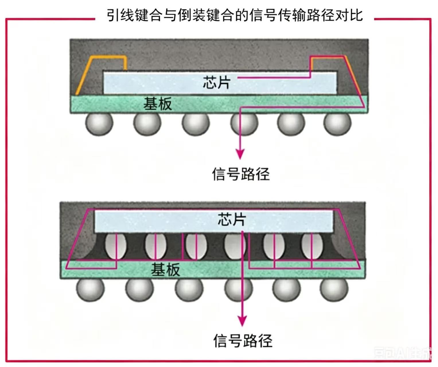
• Representative Technologies: SiP (System-in-Package) (integrating multiple chips/passive components), PoP (Package-on-Package) (vertical stacking of memory and processor), FC (Flip Chip) (chip inverted, bumps directly connecting to substrate—shortest interconnects).
• Core: Shifted from "2D tiling" to "2.5D/3D stacking," reducing volume, boosting bandwidth, and lowering power consumption, preliminarily achieving "system integration."
Stage 5: Heterogeneous Integration Era (2010s–Present) — "Advanced Packaging, Performance Ceiling Breaker"
As Moore's Law approaches physical limits, advanced packaging has become the core means of breaking through performance bottlenecks. Mainstream technologies include:
• WLP (Wafer-Level Packaging): Packaging completed directly on the wafer, offering low cost, small size, and good heat dissipation, used in mobile chips (e.g., Qualcomm Snapdragon).
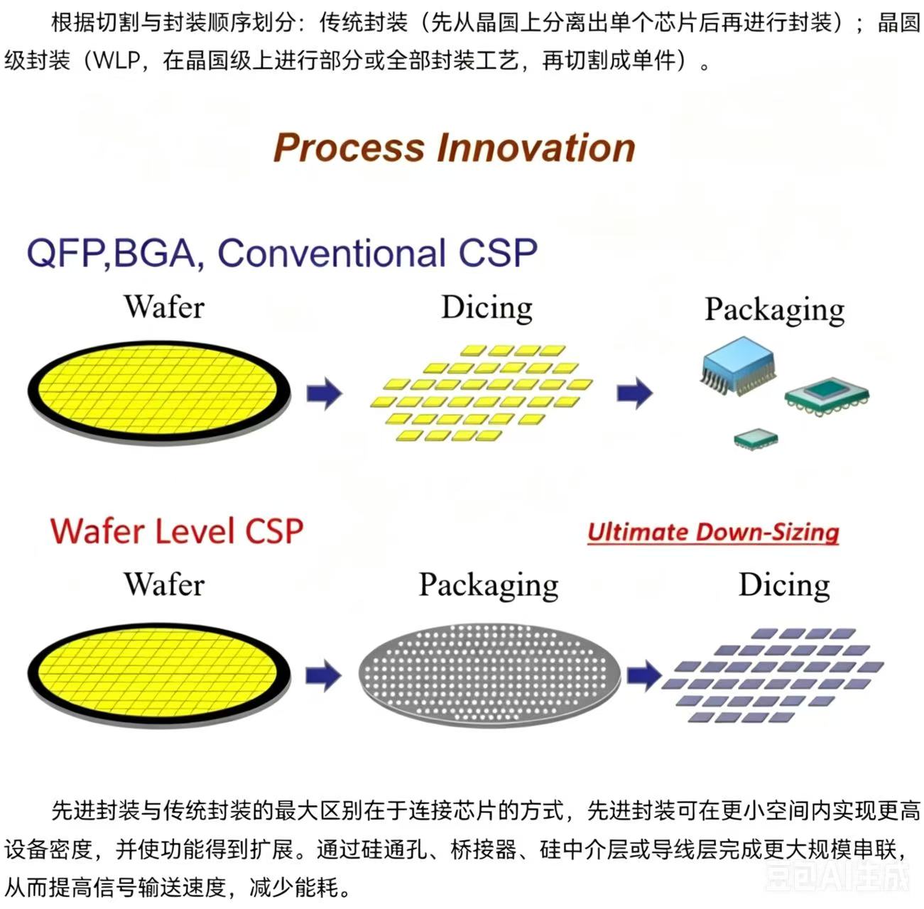
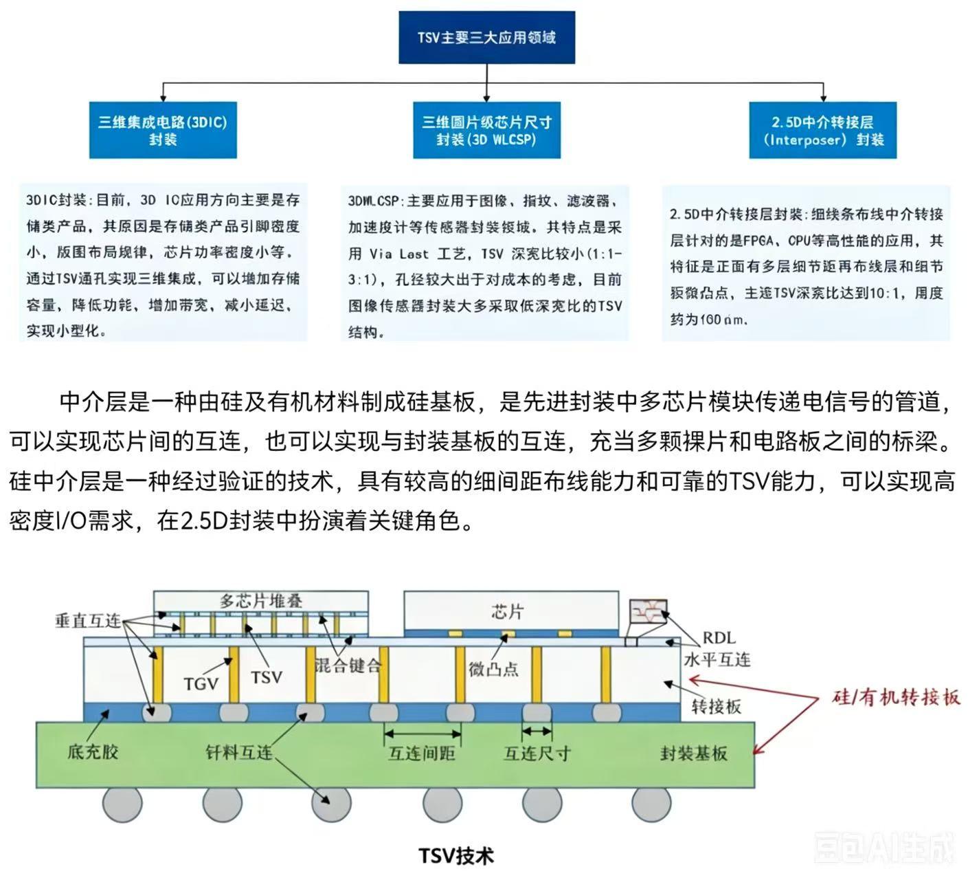
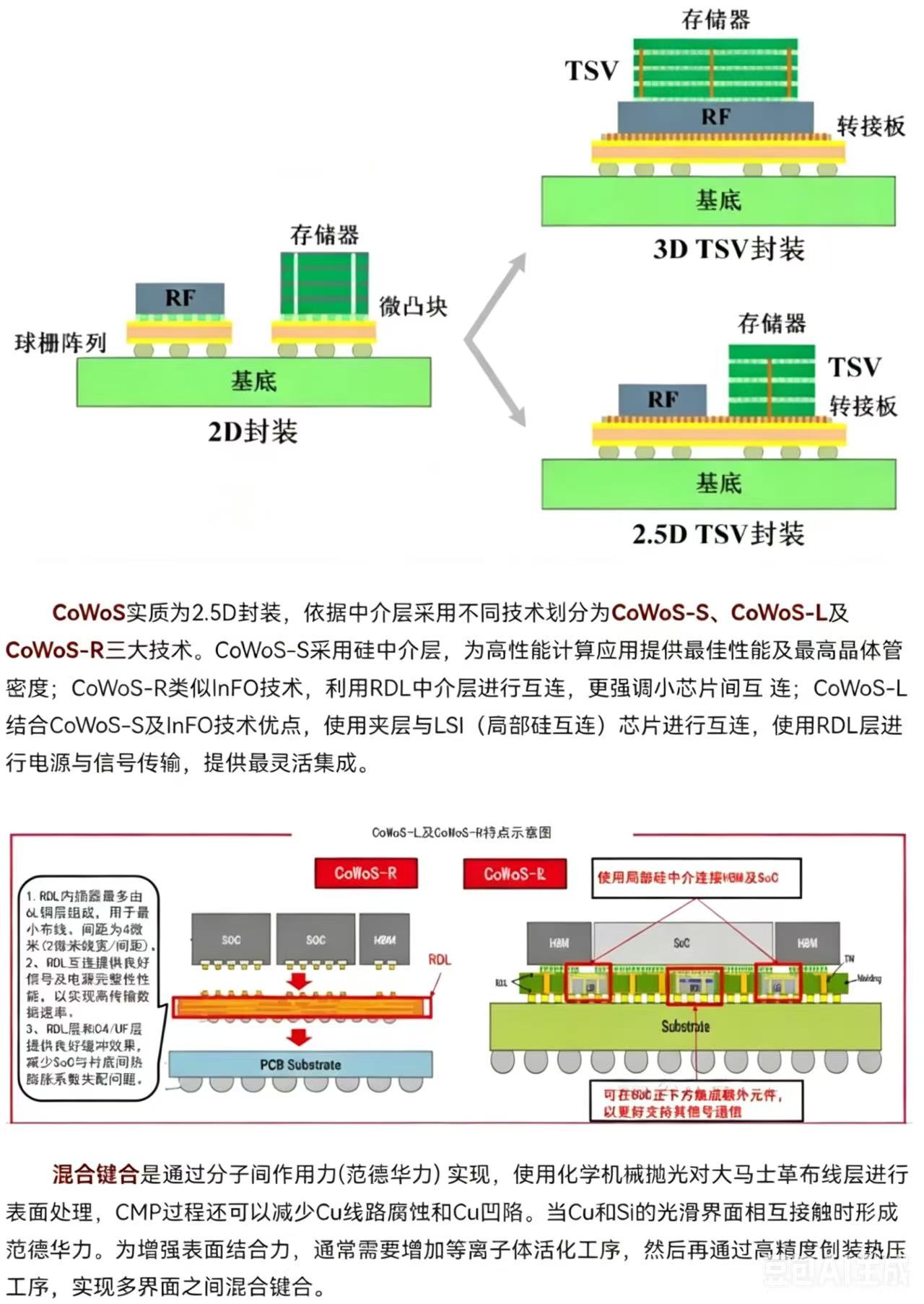
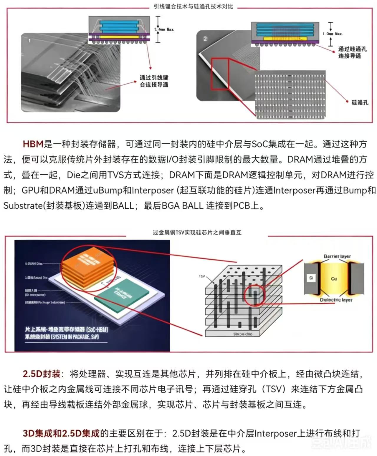
• 2.5D Packaging: Connecting multiple chips (e.g., CPU + HBM memory) via a silicon interposer + TSV (Through-Silicon Vias), offering high density, low interference, and high bandwidth, used in AI servers and high-end graphics cards.
• 3D Packaging: Chips vertically stacked, with hybrid bonding/TSV enabling direct inter-layer interconnection; interconnect length reduced to the micron scale, maximizing performance and minimizing power consumption. Representatives: TSMC CoWoS, Intel Foveros.
• Chiplet Technology: Splits a large chip into multiple "chiplets" (CPU, GPU, memory, I/O), then assembles them using advanced packaging, balancing performance, cost, and yield. This is the current mainstream approach for high-end chips (e.g., AMD Ryzen, Apple M series).
III. Comparison of Mainstream Packages: Different Scenarios, Different Choices Package Type | Core Advantage | Typical Application
• DIP: Core advantage is low cost, easy soldering; typically used in educational boards, legacy home appliances.
• QFP: Core advantage is high density, automation-friendly; typically used in general-purpose MCUs, power management chips.
• BGA: Core advantage is high pin count, strong performance; typically used in smartphone SoCs, FPGAs.
• QFN: Core advantage is ultra-thin profile, good heat dissipation; typically used in 5G RF, sensors.
• 2.5D/3D: Core advantage is ultra-high bandwidth, low power consumption; typically used in AI chips, HBM, high-end GPUs.
• Chiplet: Core advantage is flexibility, low cost, high performance; typically used in server CPUs, flagship smartphone chips.
IV. Advanced Packaging: A "Corner Overtaking" Opportunity for Domestic Chips
Currently, the global advanced packaging market is dominated by TSMC and Intel, but domestic packaging and testing companies (JCET, Tongfu Microelectronics, Huatian Technology) have risen rapidly, achieving technological breakthroughs in areas such as WLP, 2.5D, and SiP.
• Technological Breakthroughs: JCET's XDFOI, Tongfu Microelectronics' 2.5D interposer, and Huatian Technology's TSV technology are gradually narrowing the gap with international leaders.
• Industry Opportunity: The Chiplet model reduces reliance on cutting-edge process nodes; by integrating chips made with mature processes via advanced packaging, domestic chips can achieve breakthroughs in the mid-to-high-end market.
• Future Directions: Glass substrates (replacing silicon substrates, reducing costs by 50%), CPO (Co-Packaged Optics) (integrating optical modules into the package, doubling bandwidth), integrated thermal management (graphene/liquid metal cooling).
V. Conclusion: Packaging Determines the "Ultimate Height" of Chips
From DIP to 3D stacking, from "protective shell" to "performance engine," chip packaging has long ceased to be a supporting role—today, with Moore's Law slowing, advanced packaging has become the core driving force for improving chip performance.
In the future, as AI, HPC, and autonomous driving explode, packaging technology will continue evolving toward "higher integration, lower power consumption, and smaller size," and the domestic packaging and testing industry will also embrace a golden era of development amid this wave.
Shanghai Liyuan Micro Semiconductor Co., Ltd. is a professional SiP system-in-package solution development platform. For many years, we have provided customers with one-stop services and solutions, including ASIC chip design, SiP packaging design and simulation, SiP internal wafer procurement, packaging production,
system-level testing, reliability and failure analysis, and more. Our company offers free SiP/Chiplet design consultation and services to all customers, dedicated to helping clients achieve design goals such as small form factor, low power consumption,
and low cost. If interested, please feel free to contact us at +86 13817180836 (same number for WeChat).