The Essence of Chiplet
The Essence of Chiplet: Splitting Chips and Reconstructing System-Level Integration with High-Speed Interconnects
As the traditional "monolithic chip" path encounters cost and performance bottlenecks, the semiconductor industry is fully shifting toward the system-level integration era of "Chiplet + Advanced Packaging."
1. Step One: Split (Break Down into Parts)
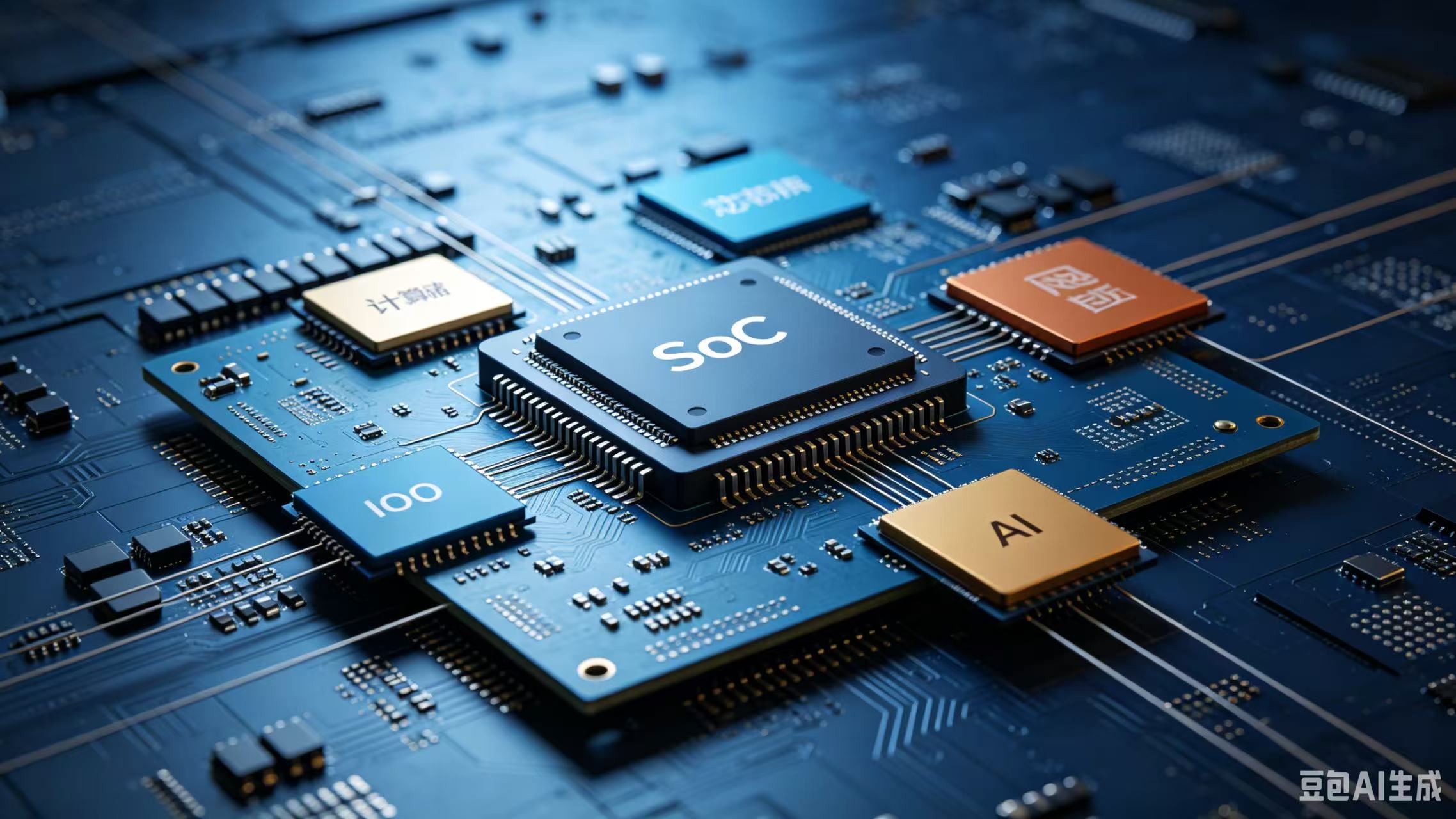
• Object: Deconstruct the traditional monolithic large-scale SoC (System-on-Chip).
• Method: Cut by functional modules (compute, memory, I/O, AI, RF, etc.), each module becoming an independent small chip (Chiplet).
• Purpose:
◦ Yield Improvement: Small chip area leads to much higher wafer yield than large chips.
◦ Process Decoupling: Different functions can use optimal process nodes (e.g., compute cores at 3nm, I/O at 22nm mature process).
◦ IP Reuse: One chiplet can be used across multiple products.
2. Step Two: High-Speed Interconnect (System Reconstruction)
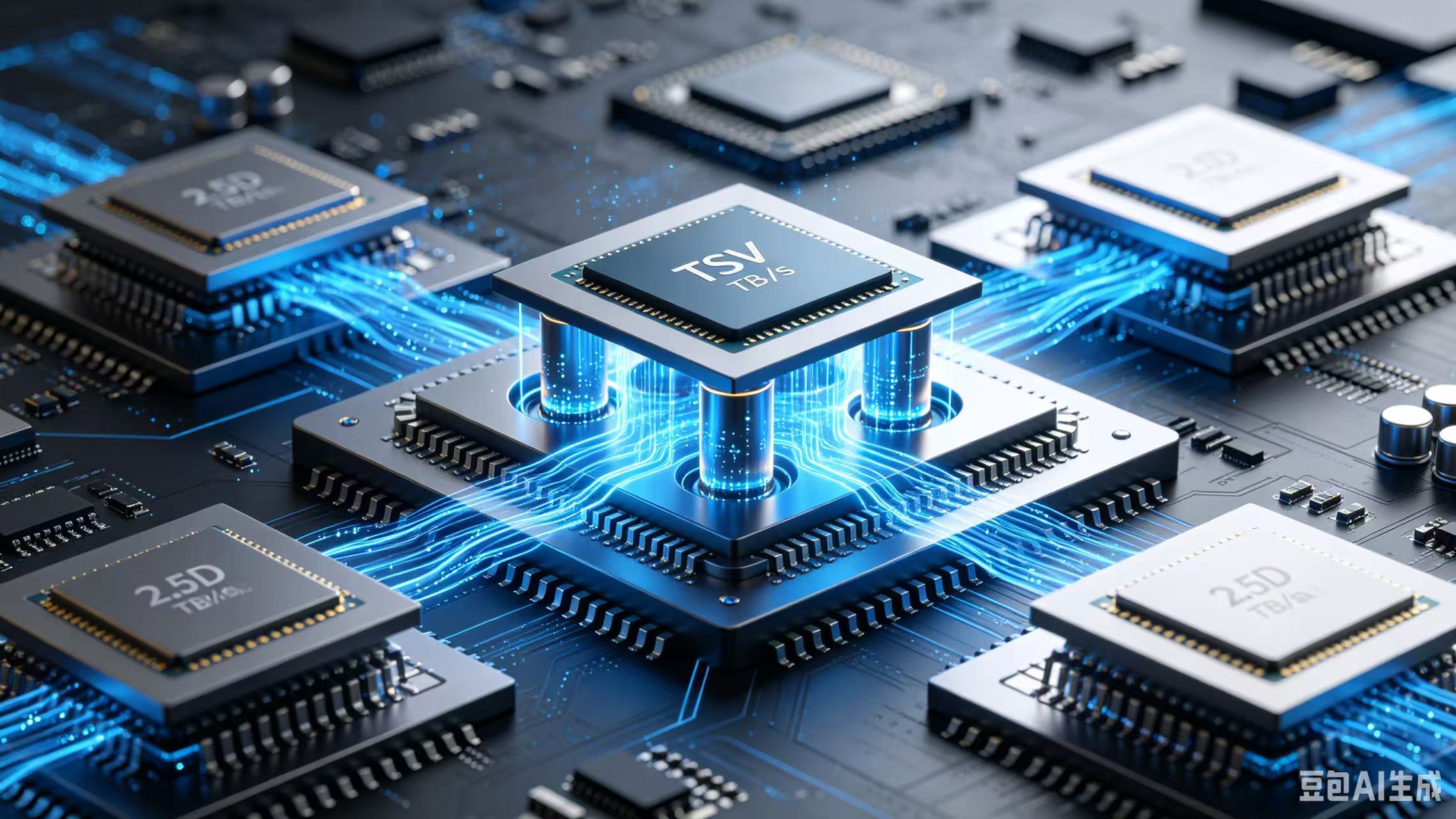
• Technology: Utilizes 2.5D/3D advanced packaging (CoWoS, EMIB, SoIC, Foveros) + TSV (Through-Silicon Via), micro bumps.
• Bandwidth: Interconnect bandwidth between chiplets can reach TB/s levels, with latency approaching on-chip bus levels.
• Standard: UCIe provides a unified interface, enabling different vendors' chiplets to be "plug-and-play."
3. Step Three: System-Level Integration (1+1>2)
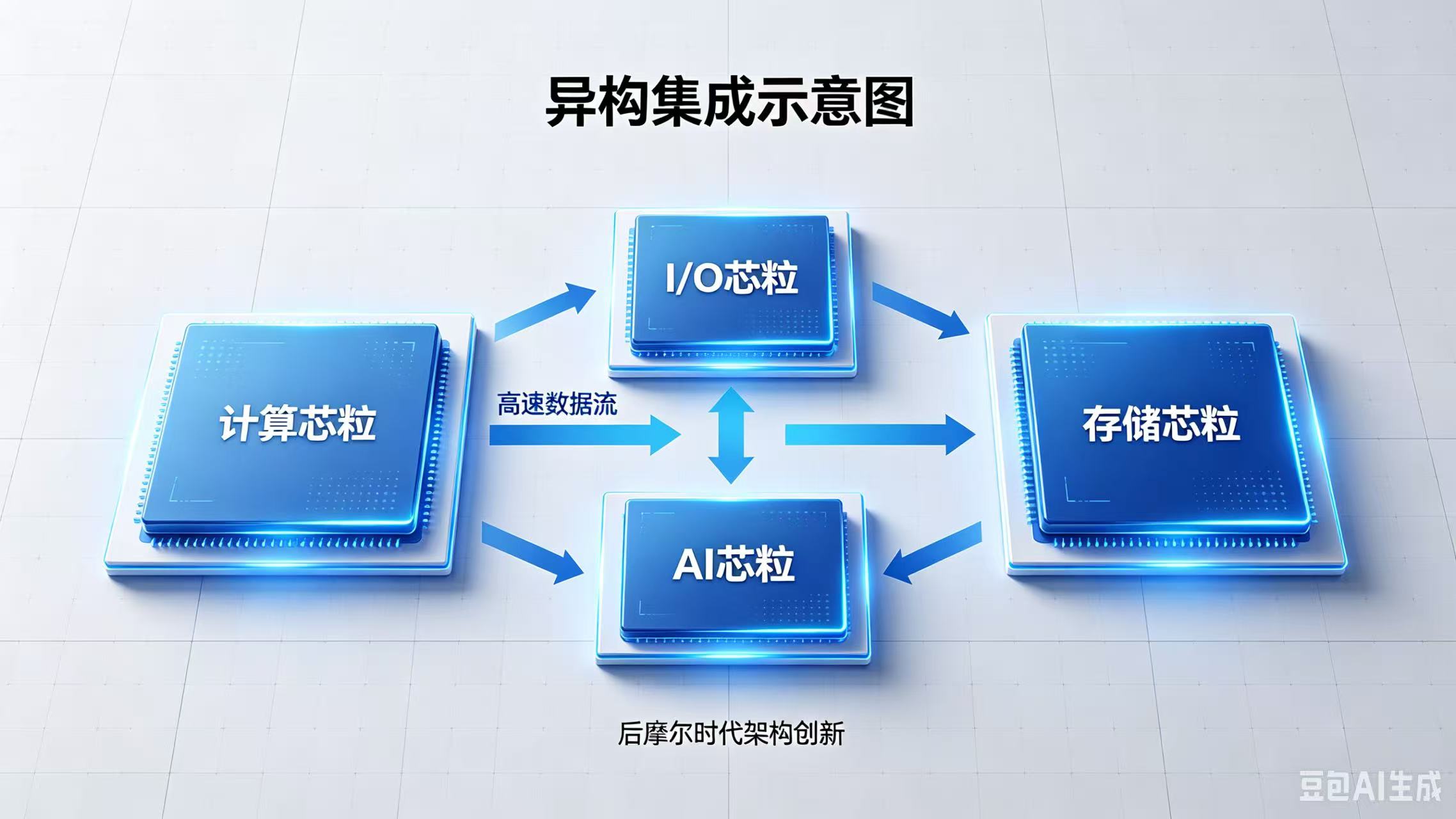
• Form Factor: Multiple heterogeneous chiplets within a single package, appearing externally as a complete chip.
• Essence: Heterogeneous integration – modules of different processes, materials, and functions collaborate at the system level.
• Value: Bypasses the physical limits of monolithic chips, extending "Moore's Law-like" performance/density improvements through architectural innovation.
Summary in One Sentence
Chiplet is: breaking large chips into small building blocks and reassembling them into a stronger system using ultra-high-speed "internal buses" – it's the Lego of chips in the post-Moore era.
Shanghai Liyuan Micro Semiconductor Co., Ltd. is a professional SiP system-level packaging solution development platform. For many years, we have provided customers with one-stop services and solutions including ASIC chip design,
SiP packaging design and simulation, wafer procurement for internal SiP use, packaging production, system-level testing, reliability and failure analysis.
Our company offers free SiP/Chiplet design consulting and services to all customers. We are dedicated to helping customers achieve design goals such as small form factor, low power consumption, and low cost.
If interested, please feel free to contact us at 13817180836 (WeChat ID same as phone number).