Frontier Breakthroughs: Five New Chip Packaging Technologies in 2026, Reshaping the Computing Power Landscape in the Post-Moore Era
As cutting-edge process nodes approach physical limits and R&D costs remain stubbornly high, chip packaging has long since evolved from a supporting process into the core engine driving chip performance gains. In 2026,
five major new technologies—Hybrid Bonding, Panel-Level Packaging (CoPoS), Glass Substrates, Co-Packaged Optics (CPO), and Chiplet Heterogeneous Integration—are accelerating from the laboratory toward large-scale mass production,
completely transforming the industry landscape for high-end chips, AI computing power, and high-speed communications.
I. Hybrid Bonding: The "Ultimate Solution" for 3D Stacking and Chiplet Interconnection
Traditional packaging relies on solder balls and copper bumps for chip interconnection, encountering bottlenecks such as large pitch, high loss, and poor heat dissipation. Hybrid Bonding abandons all solder balls and bumps, achieving direct copper-to-copper atomic-level bonding, and is the core foundational technology in the current advanced packaging field.
It compresses interconnect pitch from the traditional 10 microns to within 1 micron, boosting interconnect density by over 10 times, reducing signal latency and power consumption by over 30%, while simultaneously greatly enhancing heat dissipation capability. This technology has now become the standard process for 3D chip stacking, HBM (High Bandwidth Memory), and Chiplet integration, and is regarded as the "crown jewel" of advanced packaging. Companies like AMD, Intel, and TSMC have all completed mass production deployments, with domestic packaging and testing manufacturers also rapidly catching up.
II. CoPoS Panel-Level Packaging + Glass Substrate: Breaking the Dual Bottlenecks of Size and Cost
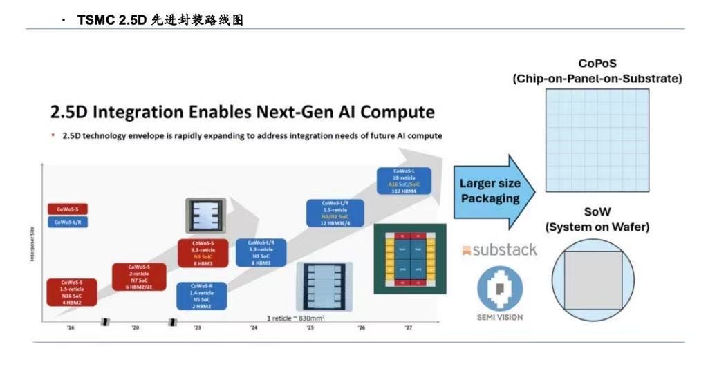
AI high-computing-power chips impose unprecedented demands on packaging area and wiring density. Traditional CoWoS silicon interposer packaging is limited by the round wafer, achieving only about 45% area utilization, along with high costs and susceptibility to warping. The combination of CoPoS (Chip-on-Panel-on-Substrate) and glass substrates has become the mainstream route for next-generation large-scale AI chips.
CoPoS replaces the round silicon wafer with a square glass panel, raising area utilization to 81% and supporting ultra-large chips with a single package area of up to tens of thousands of square millimeters, perfectly matching multi-chiplet, multi-HBM stacked architectures. Glass substrates, with their strong thermal stability, low dielectric loss, and high flatness, not only solve the warping problem of large-size packages but also support high-density wiring below 2 microns, with long-term costs approximately 50% lower than silicon interposers. 2026 is recognized within the industry as the inaugural year of glass substrate commercialization, with TSMC, Samsung, and Intel all having laid out pilot lines and mass production plans.
III. Chiplet Heterogeneous Integration: The Mainstream Architecture That Bypasses Process Barriers
Chiplet technology no longer pursues a "single monolithic chip," but instead dismantles different functional modules such as processors, memory, interfaces, and RF into independent small chips, manufactured separately using optimal processes, and then integrated into a single system through advanced packaging.
This technology significantly improves chip yield, shortens R&D cycles, and reduces the reliance of high-end chips on extreme process nodes, enabling the mixing and matching of chips with different processes, materials, and functions. The industry has now established a unified interconnect standard (UCIe), with next-generation AI chips and high-end processors from companies like NVIDIA, AMD, and Huawei fully adopting the chiplet architecture. As Moore's Law slows down, Chiplet has become the most cost-effective and fastest-to-implement technology route in the global semiconductor industry.
IV. CPO (Co-Packaged Optics): The Bandwidth Revolution for AI Data Centers
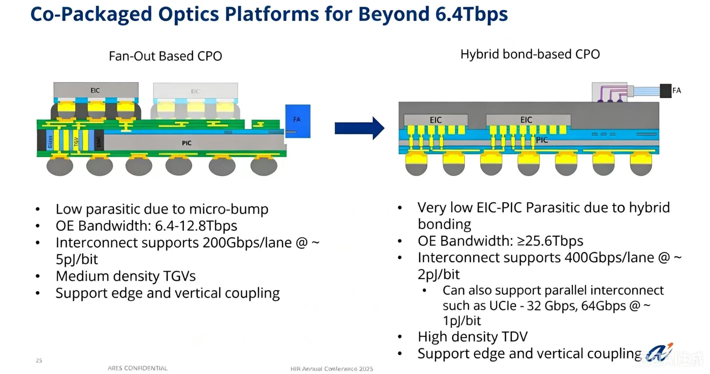
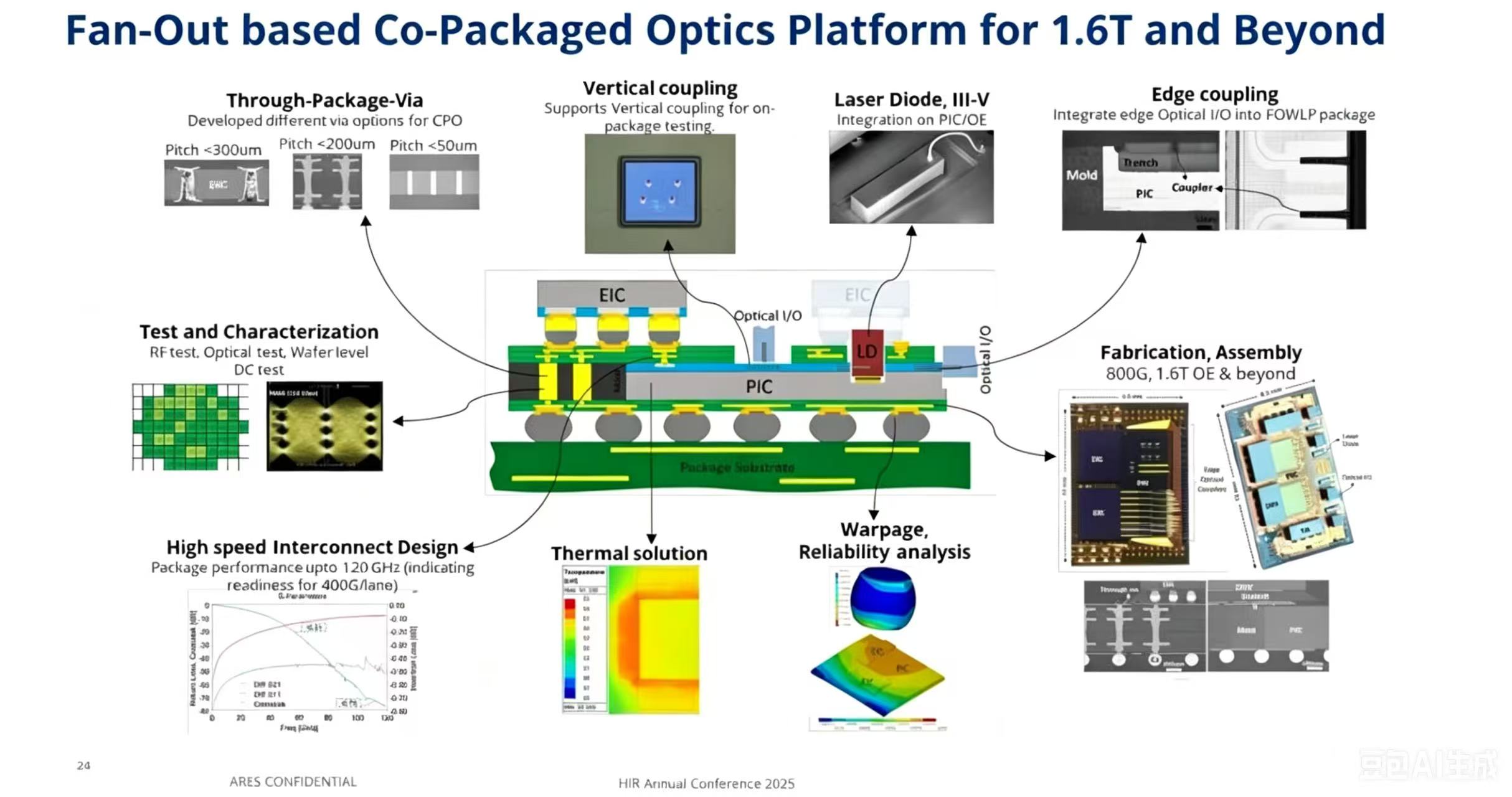
AI servers and high-speed switches face the "ceiling of electrical interconnect bandwidth," with traditional external optical modules suffering from high power consumption, high latency, and lengthy links. CPO (Co-Packaged Optics)
integrates optical engines and photonic chips directly inside the chip package, replacing electrical signals with optical signals for high-speed data transmission.
CPO compresses signal transmission distance to the millimeter scale, reduces single-channel power consumption to 2pJ/bit, and achieves bandwidths up to 25.6Tbps, multiplying bandwidth several times over while cutting power consumption by more than half compared to traditional solutions.
According to the industry roadmap, 2026–2027 will mark the inflection point for CPO mass production, becoming a standard technology for AI data centers and high-speed communication equipment. Companies like NVIDIA, AMD, and ZTE have already completed technology verification and product planning.
V. 3D Logic Folding and High-Density Fan-Out Packaging: Dual Upgrades in Miniaturization and Computing Density
1. 3D Logic Folding
Building upon 2.5D side-by-side interconnection, 3D vertical stacking achieves layer-by-layer chip stacking through TSV (Through-Silicon Vias) and Hybrid Bonding. Huawei's proposed "Tao's Law" specifically positions logic folding as a core path for performance improvement.
This technology exponentially increases computing density within limited space and shortens interconnect paths. It has already been applied to cache stacking and AI computing chips, becoming an important means for mature processes to achieve high-end performance.
2. Next-Generation High-Density Fan-Out Wafer-Level Packaging (FOWLP)
Fan-Out Wafer-Level Packaging requires no traditional substrate, completing wiring and packaging directly on the wafer. With its advantages of thin profile, low cost, and high I/O density, it continues to iterate and upgrade. In 2026, multi-chip fan-out and ultra-high-density fan-out solutions are being fully popularized, widely used in mobile phone main chips, RF modules, and wearable devices, balancing miniaturization, high performance, and mass production cost.
VI. Overall Trends in New Technology Development
1. From "Single Packaging" to "System-Level Integration"
Packaging is no longer merely a shell and interconnection; it is a system-level solution integrating computing, storage, optoelectronics, and thermal management. Packaging and testing companies are gradually transforming into technology solution providers.
2. Three Major Transformations Advancing in Parallel: Materials, Architecture, and Optoelectronics
Substrates are iterating from silicon and organic materials toward glass; architecture is moving from 2D to 2.5D/3D and panel-level; interconnects are evolving from purely electrical to optoelectronic fusion. These three directions mutually empower one another.
3. Coexistence of Advanced and Traditional Packaging in a Layered Market
High-end AI, computing power, and communication chips will centrally adopt the five major new technologies mentioned above; traditional DIP, QFP, and conventional BGA, leveraging their cost advantages, will continue to deeply cultivate markets such as consumer electronics, industrial control, and home appliances, forming a differentiated landscape.
Conclusion
In 2026, chip packaging has officially entered a technology explosion phase. The five major new technologies—Hybrid Bonding, CoPoS + Glass Substrates, Chiplet, CPO, and 3D Stacking—jointly open up room for performance growth in the post-Moore era. Over the next 5–10 years, the primary battleground of chip competition will gradually shift from wafer manufacturing toward advanced packaging and system integration. For the domestic semiconductor industry, this represents both a major opportunity to narrow the gap and a core track that must be tackled with full effort.
Shanghai Liyuan Micro Semiconductor Co., Ltd. is a professional SiP system-in-package solution development platform. For many years, we have provided customers with one-stop services and solutions, including ASIC chip design, SiP packaging design and simulation, SiP internal wafer procurement, packaging production, system-level testing,
reliability and failure analysis, and more. Our company offers free SiP/Chiplet design consultation and services to all customers, dedicated to helping clients achieve design goals such as small form factor, low power consumption, and low cost.
If interested, please feel free to contact us at +86 13817180836 (same number for WeChat).