From SoC → SoIC → CIC
The transition from SoC → SoIC → CIC represents the technological evolution of chips from 2D planar integration to 3D立体 integration, and ultimately to full-space cubic integration. The core objective is to break through the limits of Moore's Law, pursuing higher density, stronger performance, and lower power consumption.
1. SoC (System on Chip) – The 2D Planar Era
Definition:
A single-chip system where all functional modules, including CPU, GPU, memory, interfaces, and controllers, are integrated onto a single silicon die.
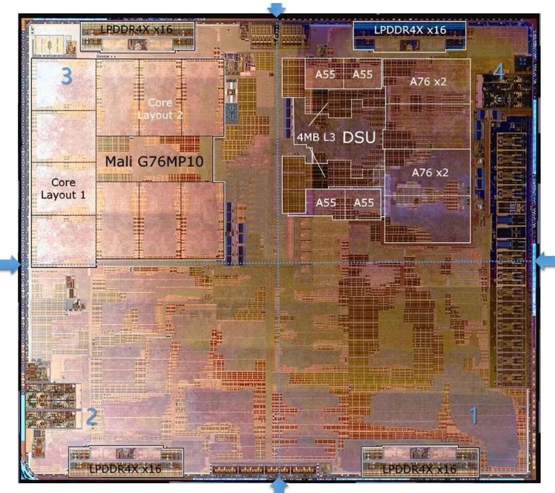
Characteristics:
• Planar integration: Only a single layer of transistors
• Uniform process manufacturing: All IPs must use the same process generation (e.g., 5nm)
• Advantages: Low latency, simple structure, mature and stable
• Bottlenecks:
◦ Process technology approaches physical limits, costs skyrocket
◦ Different modules (logic/memory/analog) are difficult to optimize with a single process
◦ Trade-offs between area, power consumption, and yield are hard to balance
2. SoIC (System on Integrated Chips) – The 3D Stacking Era
Definition:
A 3D advanced packaging technology proposed by TSMC. It vertically stacks multiple chiplets of different functions and process nodes using bumpless hybrid bonding.
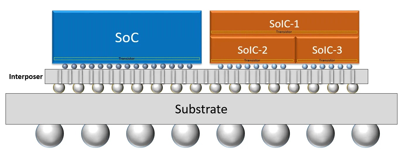
Core Advantages:
• Heterogeneous integration: Logic (7nm) + Memory (12nm) + Analog (28nm) can be freely combined
• Bumpless bonding: Signal density reaches ~14,000/mm², approaching on-die levels
• 3D stacking: Multiple dies stacked vertically, doubling transistor count within the same footprint
• Low latency, low power: Signal paths are drastically shortened
Two Forms:
• WoW (Wafer-on-Wafer): Whole-wafer to wafer bonding (high precision, high efficiency)
• CoW (Chip-on-Wafer): Known Good Dies (KGD) attached to a wafer (better yield control)
3. CIC (Cubic Integrated Circuit) – The Full 3D Cubic Era
Definition:
A more advanced concept: a truly three-dimensional chip. It is not simply "stacking" layers, but rather a design where transistors and interconnect networks are evenly distributed throughout the entire volume of a "cube," with立体布线 in the X, Y, and Z directions.
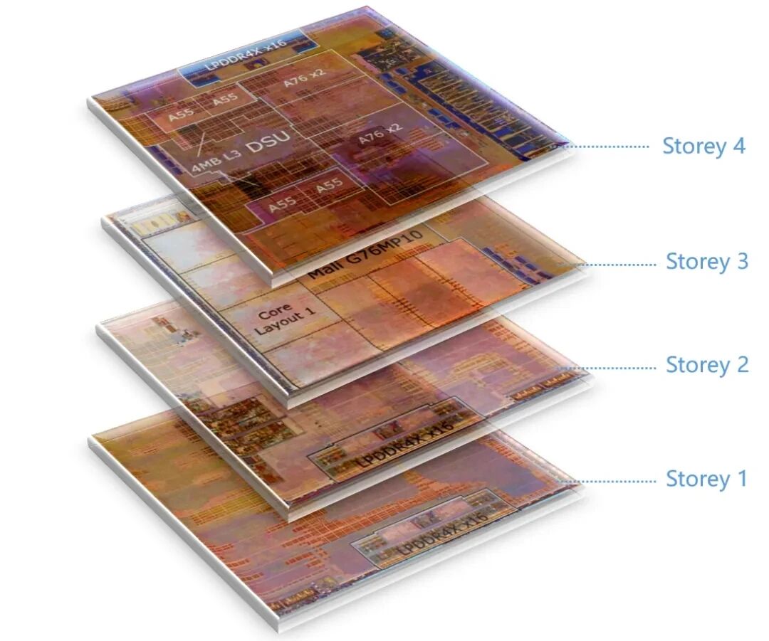
Core Concept:
• From a "planar board" to a true "chip cube"
• Shorter interconnects, better heat dissipation, higher density
• Breaks through the bottlenecks of 2D routing congestion and the thermal wall
• Currently still in the conceptual/R&D phase, representing the long-term direction of the post-Moore era
If CIC can be realized, the world's largest chip today, the plate-sized WSE (Wafer Scale Engine) with 2.6 trillion transistors, could, according to the CIC design concept, be completely implemented within a fingertip-sized 1 cubic centimeter.
Comparison of the Three:
• SoC: One wafer, one layer of function, single process → 2D single chip
• SoIC: Multiple small chips, vertical stacking, heterogeneous processes → 3D packaging integration
• CIC: Full 3D cube, spatial立体 design → Ultimate 3D chip form
Shanghai Liyuan Micro Semiconductor Co., Ltd. is a professional SiP system-level packaging solution development platform. For many years, we have provided customers with one-stop services and solutions including ASIC chip design,
SiP packaging design and simulation, wafer procurement for internal SiP use, packaging production, system-level testing, reliability and failure analysis.
Our company offers free SiP/Chiplet design consulting and services to all customers. We are dedicated to helping customers achieve design goals such as small form factor, low power consumption, and low cost.
If interested, please feel free to contact us at 13817180836 (WeChat ID same as phone number).