Three Major Technology Trends Driven by Chiplet
Three Major Technology Trends Driven by Chiplet: When Silicon-Based Life Learns to Grow Like Building Blocks
On September 12, 1958, the gentle giant Jack Kilby invented the integrated circuit. At the time, no one knew how profoundly this invention would change the human world.
Forty-two years later, Kilby received the 2000 Nobel Prize in Physics for inventing the integrated circuit. "Laid the foundation for modern information technology" was the apt assessment given by the Nobel Committee.
The progress of science and technology is often driven by a series of dreams, and the integrated circuit is certainly no exception.
The dream of Kilby – a two-meter-tall, gentle and steady TI engineer – was "to use a single semiconductor material to fabricate all the devices needed for a circuit."
Seven years after the invention of the integrated circuit, Intel co-founder Gordon Moore proposed his prophetic dream: "The number of devices on an integrated circuit will double approximately every eighteen months." This is what we know today as Moore's Law.
In the end, both realized their dreams, driving tremendous technological progress. The superposition of these two great dreams has also shaped the semiconductor industry as we know it today.
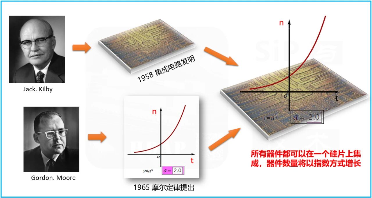
As the pace of Moore's Law gradually slows before the physical limits of the nanometer scale, and as the complexity of a single chip climbs an insurmountable Everest, the semiconductor industry has not fallen into silence. Instead, in a wiser and gentler way,
it has begun a magnificent transformation in the post-Moore era. Chiplet technology, like a gentle revolution, has transformed cold silicon dies into magical building blocks that can be freely combined,
bringing three profound and perceptible technological trends to the world of chips.
I. IP as Chiplet: From Intangible Code to Tangible Silicon Soul
Once upon a time, chip design was a solitary ascetic practice. Engineers, lost in the labyrinth of billions of transistors, condensed their wisdom into lines of Verilog code, ultimately solidifying it into a complete SoC (System-on-Chip).
Those exquisite functional modules, such as CPU cores and interface protocols, existed only as intangible IP cores – crystallized wisdom residing in drawings and simulations, unable to breathe independently.
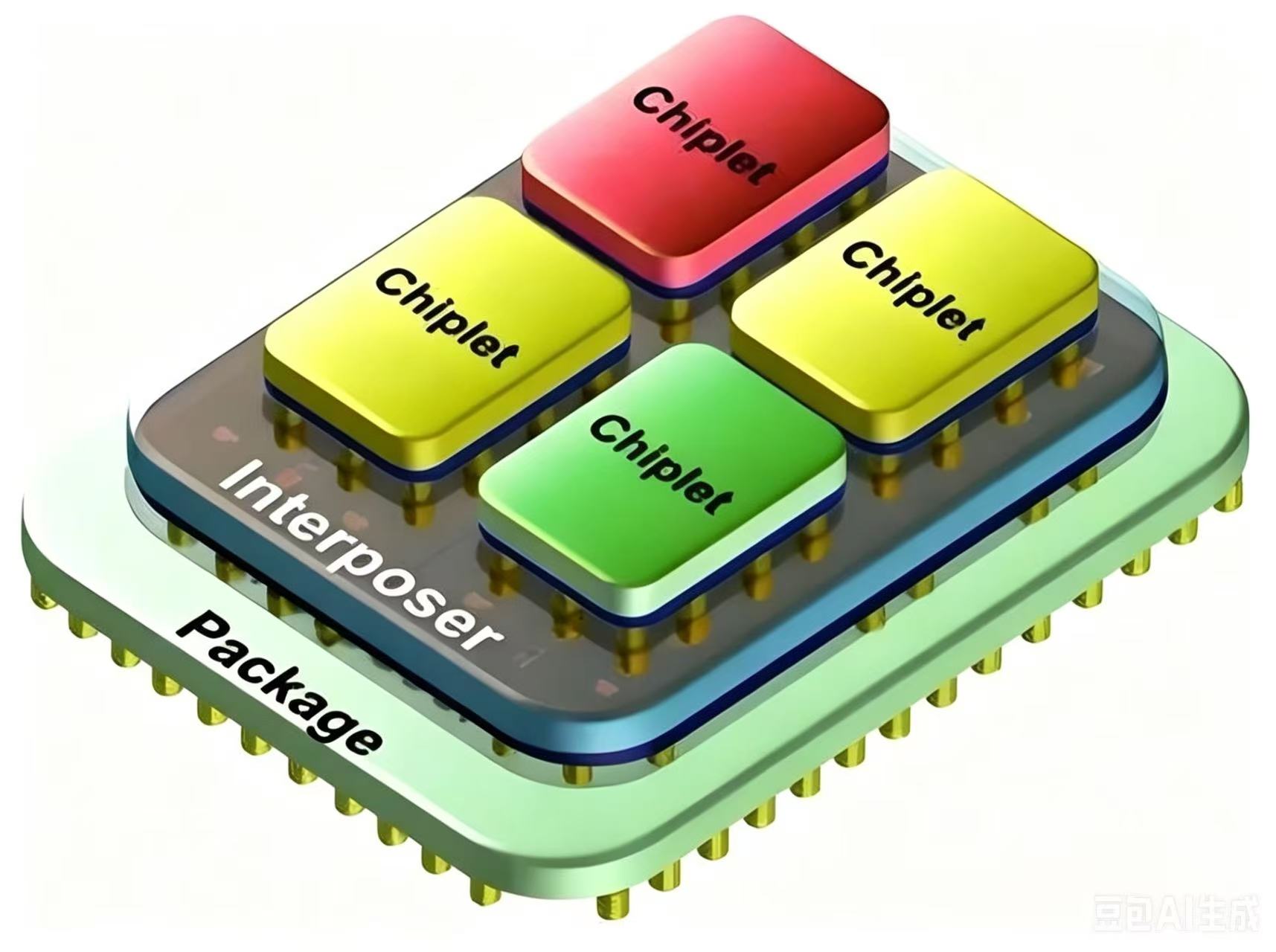
The arrival of Chiplet has fundamentally changed this. IP as Chiplet is the first gentle transformation. It has forged those once-abstract, intangible intellectual property rights
from the virtual world of code into tangible, independently manufacturable "small chips."
These are no longer mere design modules on paper, but silicon souls with physical form. A USB controller, an NPU compute unit, a high-speed interface – each can be an independent chiplet.
They are carefully manufactured, rigorously tested, possessing their own process technology, their own lifespan, their own value. This means that wisdom can be encapsulated, reused, and traded.
Just as human civilization turned knowledge into books, Chiplet has cast the wisdom of hardware into silicon-based movable type that can circulate and be passed down.
From now on, innovation is no longer a solitary battle starting from zero, but a free combination standing on the shoulders of countless mature "chiplets," allowing every inspiration to be realized faster.
II. Heterogeneous Integration: Breaking Down the Walls of Process, Embracing Diverse Symbiosis
The traditional chip world was a rigid "one-size-fits-all" kingdom. To be integrated on the same wafer, all functions – whether it's logic computing pursuing extreme performance, or analog interfaces requiring stability and reliability – had to succumb to the same process node.
This is like forcing a sprinter and a painter to use exactly the same training methods and tools, often leading to compromises and high costs.
The second trend brought by Chiplet, heterogeneous integration, has completely shattered this wall that禁锢ed creativity. It declares: Everything can be interconnected; they don't have to share the same origin.
Thus, we see a diverse, symbiotic silicon-based utopia: CPU cores pursuing ultimate computing power can unabashedly adopt the most cutting-edge 3nm process, squeezing out every bit of performance;
I/O interfaces responsible for external connections and analog circuits for power management can comfortably use mature, stable, low-cost 28nm processes.
Even more, storage and computing can be brought close together, AI accelerators and general-purpose processors can embrace seamlessly, and photonic chips and electronic chips can coexist under one roof.
This is a philosophy of "harmony without uniformity." Each chiplet grows in the soil best suited for it, exists in its optimal form, and then, through advanced packaging technology, achieves the most efficient collaboration within a kingdom the size of a square inch.
This boundary-breaking integration means chips are no longer the compromised product of a single process, but a super-organism that gathers the strengths of many, finding for the first time such a perfect balance between performance and cost, speed and power consumption.
III. Interconnect Standardization: From Isolated Islands to an Open Silicon-Based Continent
The greatness of technology often lies not in极致 performance, but in the ability to establish an open, inclusive ecosystem. The third, and most far-reaching, trend brought by Chiplet is interconnect standardization.
If Chiplets are high-tech building blocks, then without a unified interface standard, they are just a pile of loose sand, each manufacturer having its own unique凹凸, unable to communicate.
The emergence of standards like UCIe (Universal Chiplet Interconnect Express) is like establishing a unified "language" and "law" for the silicon-based world.
It defines a high-speed, low-latency, low-power way for chiplets to communicate, allowing chiplets from different manufacturers, different processes, and different functions
to "shake hands" and "converse" without barriers.
This means an unprecedented open ecosystem is budding. The future chip world will no longer be the closed, vertical kingdoms of giants, but a freely thriving silicon-based continent.
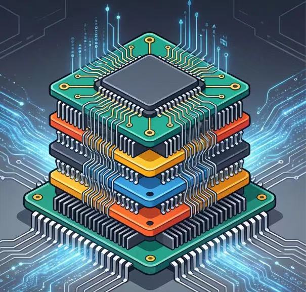
Specialized chiplet suppliers can focus on refining their own best-in-class modules, while system designers can freely pick and choose various standardized "parts" like CPU, GPU, memory, and interfaces, as if shopping in a supermarket,
to quickly assemble customized chips that meet ever-changing needs, just like building with Legos.
This is a paradigm shift from "closed manufacturing" to "open innovation." It lowers the barriers to entry, inspires diverse creativity, and moves the semiconductor industry from the niche self-admiration of high-tech
towards a collaborative evolution that benefits everyone. Every small chiplet is no longer isolated; they are connected through a unified bond into a digital future of infinite possibilities.
Conclusion: A New Childhood for Silicon-Based Life
These three major trends brought by Chiplet – IP as Chiplet, heterogeneous integration, and interconnect standardization – are essentially an intelligent evolution of chip technology from the brute-force approach of "making it bigger and stronger" to "division of labor and collaboration."
It gives cold silicon dies a living spirituality: from intangible to tangible (IP as Chiplet) is the embodiment of the soul; from single to diverse (heterogeneous integration) is the liberation of the individual;
from closed to open (standardization) is the rise of a civilization.
This is not just a technological iteration, but a philosophical revolution about integration, symbiosis, and creation. Under the starlight of the post-Moore era, Chiplet, with its unique gentleness and power,
tells us: When faced with physical limits, the boundless possibilities of thought are the eternal vitality of technology. We are witnessing silicon-based life entering a brand new childhood of building-block-like growth and free combination.
Shanghai Liyuan Micro Semiconductor Co., Ltd. is a professional SiP system-level packaging solution development platform. For many years, we have provided customers with one-stop services and solutions including ASIC chip design,
SiP packaging design and simulation, wafer procurement for internal SiP use, packaging production, system-level testing, reliability and failure analysis.
Our company offers free SiP/Chiplet design consulting and services to all customers. We are dedicated to helping customers achieve design goals such as small form factor, low power consumption, and low cost.
If interested, please feel free to contact us at 13817180836 (WeChat ID same as phone number).