The Ideal of Genius Lost to the Embrace of Reality – Why HMC Lost to HBM
HMC (Hybrid Memory Cube) and HBM (High Bandwidth Memory) both once aimed to replace DDRx. Similar in name and structure, and both enhanced by 3D TSV technology, their performance far exceeded that of DDRx memories of the same era. Driven by the AI wave, HBM is now at its peak, while HMC has quietly faded away. What caused such a huge difference?
There were once two genius contenders in the memory world, both hoping to break the "planar cage" of traditional memory and build data "skyscrapers" using 3D stacking. One was HMC (Hybrid Memory Cube), which debuted earlier and was more technologically aggressive, like an aloof genius;
the other is HBM (High Bandwidth Memory), which progressed steadily and knew how to compromise, like a pragmatic partner. In the end, HMC faded away amidst applause, while HBM became the "golden blood" of the AI era.
I. HMC: Born Ahead of Its Time, Yet Living in Lofty Ideals
In 2011, Micron led the launch of HMC, which amazed the world from the start – its bandwidth was 15 times that of DDR3, and its energy efficiency crushed all competing memories of the time.
Its design was just too "extreme": it sealed memory and control logic inside a single "cube," using high-speed serial links for transmission, like building a supercar for a closed track – maximizing performance, but incompatible with any ordinary road.
• Too aloof, unwilling to integrate with the world
HMC insisted on its own closed standards, only forming a small consortium (HMCC) with a few manufacturers, refusing to join the industry's common JEDEC family.
It thought, "I am the strongest; the world should adapt to me," forgetting that the semiconductor industry has never been about "winner takes all," but about ecosystem symbiosis.
• Too aggressive, failing in both cost and compatibility
Its structure was complex, the process extremely difficult, and the cost prohibitively high; although its serial interface was fast, it clashed with the "temperament" of GPUs and CPUs – higher latency, stiff interaction, unable to work "intimately" with compute chips.
It was like a perfect laboratory artwork, impossible to mass-produce or popularize, only able to admire itself in niche corners like supercomputing.
II. HBM: Not the Most Dazzling, But the Most Suitable
In 2013, AMD and Hynix launched HBM. It didn't have earth-shattering specs, but it caught the pulse of the times.
It took a 3.5D packaging approach: using a silicon interposer to tightly "bind" the memory stack and GPU/CPU together on the same substrate.
• Knew how to compromise and embrace the ecosystem
HBM joined JEDEC as soon as it was born, becoming a global standard. It didn't create a closed system but opened itself up to all manufacturers – NVIDIA, AMD, Samsung, SK Hynix all joined in, turning from a solo dance into a chorus involving everyone.
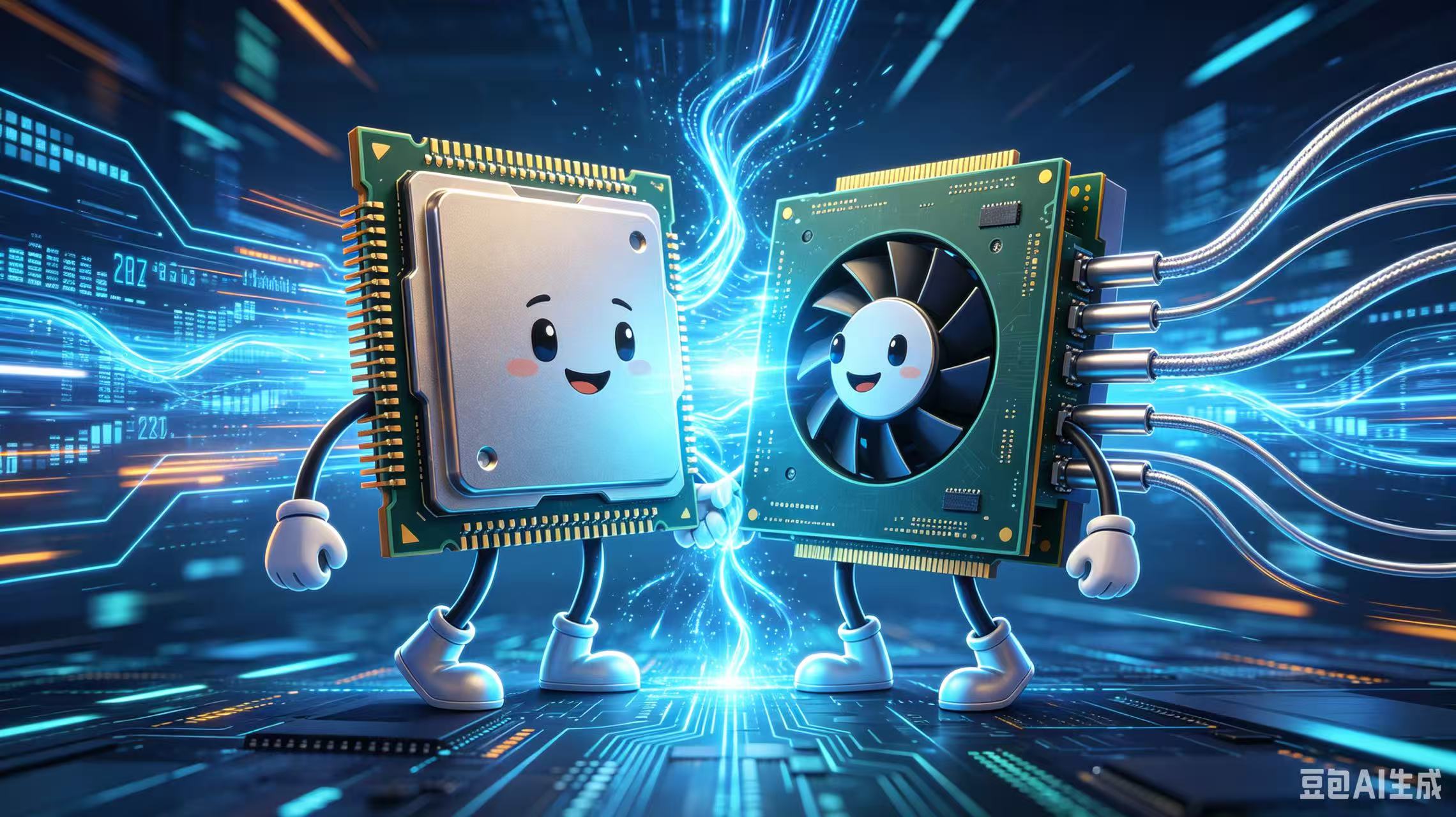
• Knew how to be pragmatic, aligning with the true needs of AI and GPUs
It used an ultra-wide parallel interface, resulting in lower latency and smoother collaboration with compute chips; it was smaller and more power-efficient, fitting perfectly into graphics cards and AI accelerators.
When AI exploded and GPUs needed to be "fed" massive amounts of data, HBM happened to be perfectly positioned to provide a close-coupled supply – not the absolute strongest in performance, but the "understanding companion" that best knew the needs of computing power.
III. The Truth of Defeat: Ideals Lost to Real-world Compromises, Aloofness Lost to Warmth
HMC lost because it was too perfect, too ahead of its time, too lonely:
• It pursued absolute performance but neglected cost, mass production, and compatibility;
• It wanted to set the rules but was unwilling to integrate into the industry ecosystem;
• It was like a genius living in a vacuum, unwilling to accommodate the real world.
HBM won because it understood balance, practicality, and connection:
• The technology wasn't extreme, but it was just enough and worked well;
• The standard was open, allowing everyone to participate and benefit;
• It grew close to GPUs, close to AI, close to market demand, transforming from a "niche technology" into a "necessity of the era."
The battlefield of technology is never about "who is more extreme wins," but about who can better integrate into the world, serve the era, and connect with everyone.
HMC is a brilliant idealistic legend, while HBM is a warm realist victory – only those embraced by the world can ultimately change the world.
Shanghai Liyuan Micro Semiconductor Co., Ltd. is a professional SiP system-level packaging solution development platform. For many years, we have provided customers with one-stop services and solutions including ASIC chip design,
SiP packaging design and simulation, wafer procurement for internal SiP use, packaging production, system-level testing, reliability and failure analysis.
Our company offers free SiP/Chiplet design consulting and services to all customers. We are dedicated to helping customers achieve design goals such as small form factor, low power consumption, and low cost.
If interested, please feel free to contact us at 13817180836 (WeChat ID same as phone number).