What is 3.5D packaging?
3.5D packaging, simply put, is a "hybrid" of 2.5D packaging and 3D packaging.
It combines the advantages of both technologies, striking a balance between performance, heat dissipation, and cost, and is currently the mainstream high-end solution for AI/computing chips.
I. First, understand: What are 2D, 2.5D, and 3D packaging?
• 2D Packaging (Traditional)
Chips are placed side by side on a substrate, like laying out objects on a desktop.
Long interconnects, slow speed, large footprint.
• 2.5D Packaging
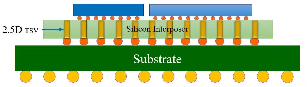
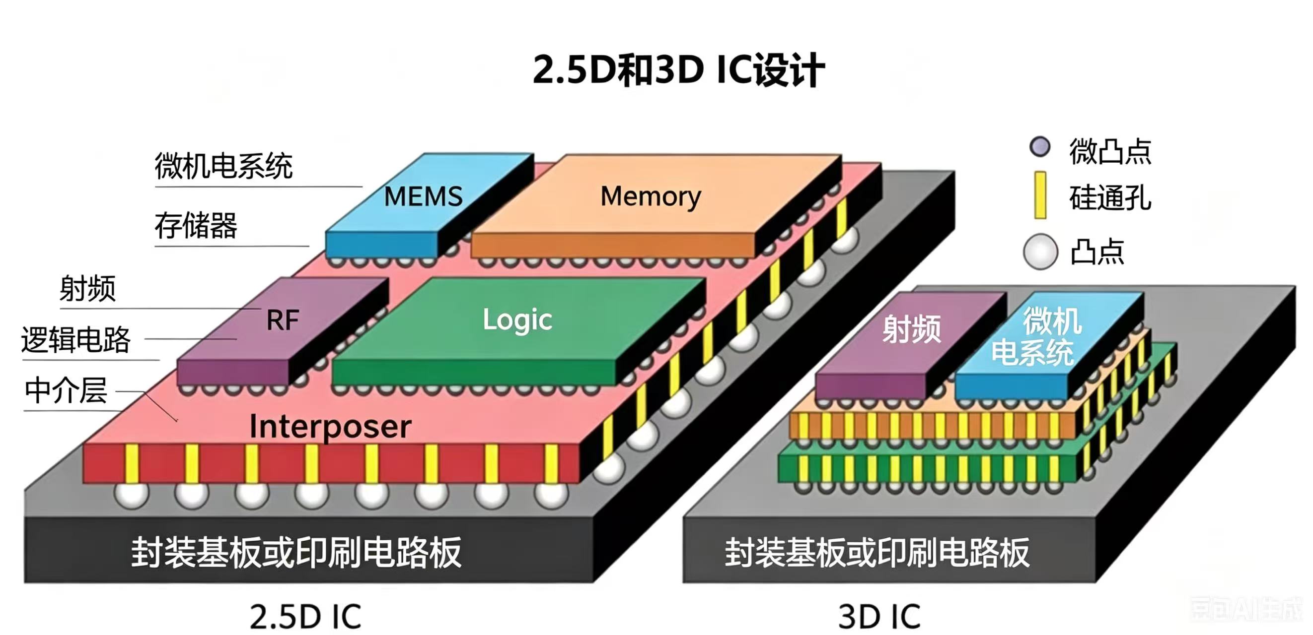
Chips are placed side by side on a silicon interposer, which contains ultra-fine wiring and TSVs (Through-Silicon Vias) for connection, then connected to the substrate.
Shorter interconnects, higher bandwidth, easier heat dissipation.
• 3D Packaging
Chips are stacked directly vertically (like stacking blocks), connected through TSVs or Cu-Cu bonding.
Smallest footprint, fastest speed, but heat is concentrated, yield is lower, and cost is high.
II. 3.5D Packaging: What does it actually look like?
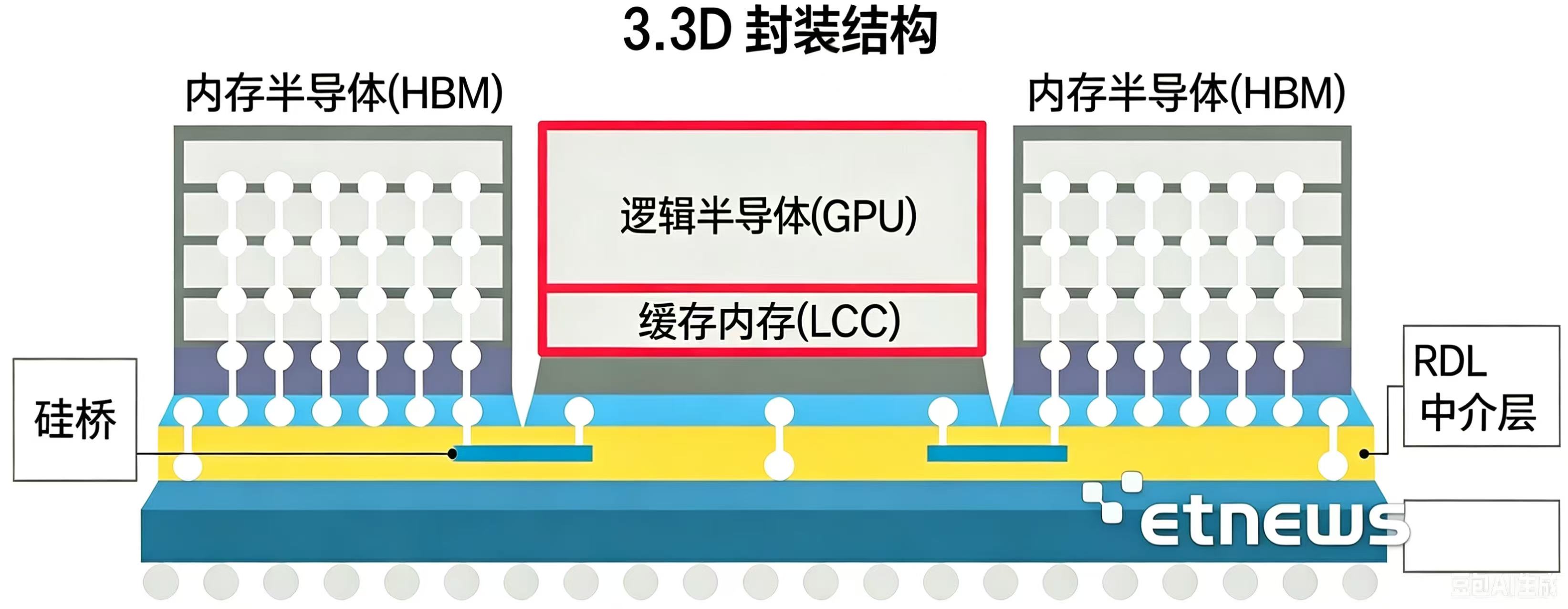
Core structure: 3D stacking within modules + 2.5D interconnects between modules.
1. First, vertically stack similar chips into small modules (the 3D part).
For example, HBM (High Bandwidth Memory) internally stacks 8 layers of DRAM.
2. Then, place these 3D modules alongside logic chips (GPU/CPU) on a silicon interposer (the 2.5D part).
3. The interposer handles high-speed interconnection and then connects to the external substrate.
In a nutshell:局部叠高高,整体排排坐。
III. What are the advantages of 3.5D? (Compared to 3D)
• More stable heat dissipation: Unlike full 3D where heat is trapped between layers, heat can be dissipated more easily.
• Higher yield: If one layer fails in a 3D stack, the whole thing is scrapped; 3.5D uses "modules + interposer," resulting in lower failure rates and controllable costs.
• Performance close to 3D: Key high-speed links (e.g., CPU-HBM) use short-range 3D direct connections, so speed is almost uncompromised.
• More mature process: Leverages existing 2.5D silicon interposer production lines, avoiding a complete equipment overhaul.
IV. Where is it used? (You've definitely heard of these)
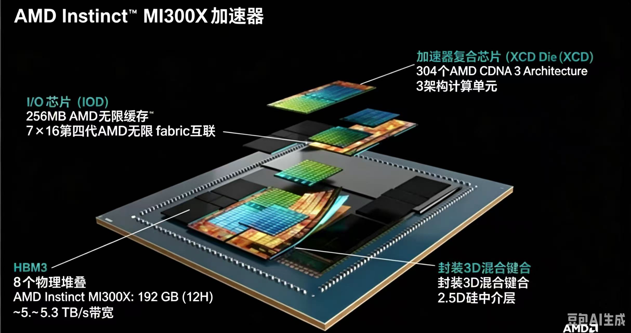
• AMD MI300 Series: GPU+CPU+HBM are co-packaged using 3.5D.
• NVIDIA H100/H200: Paired with multiple HBM units, a typical 3.5D architecture.
• Broadcom XDSiP: A 3.5D packaging platform for AI supercomputing.
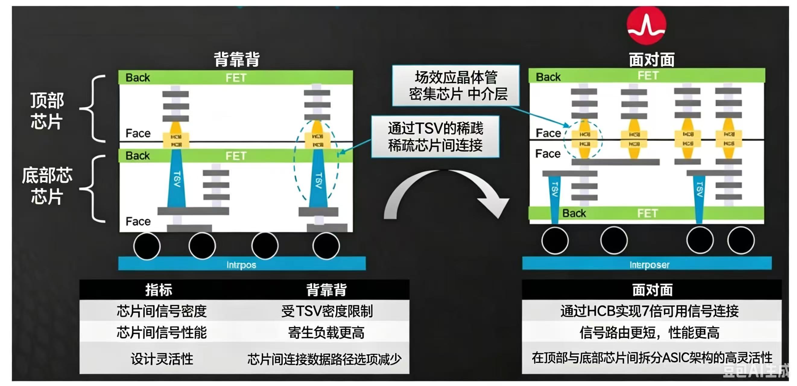
V. One-sentence summary
3.5D packaging = High performance of 3D + Good heat dissipation/yield of 2.5D.
It is not a transition but rather the most practical "golden architecture" for today's high-end chips.
Shanghai Liyuan Micro Semiconductor Co., Ltd. is a professional SiP system-level packaging solution development platform. For many years, we have provided customers with one-stop services and solutions including ASIC chip design,
SiP packaging design and simulation, wafer procurement for internal SiP use, packaging production, system-level testing, reliability and failure analysis.
Our company offers free SiP/Chiplet design consulting and services to all customers. We are dedicated to helping customers achieve design goals such as small form factor, low power consumption, and low cost.
If interested, please feel free to contact us at 13817180836 (WeChat ID same as phone number).